Lab 7 - EE 421L 

Authored by Jeeno Doria,\

doriaj3@unlv.nevada.edu

11/07/2017


Lab description: Cover all of the basic building blocks used in an ALU.


PreLab:

   
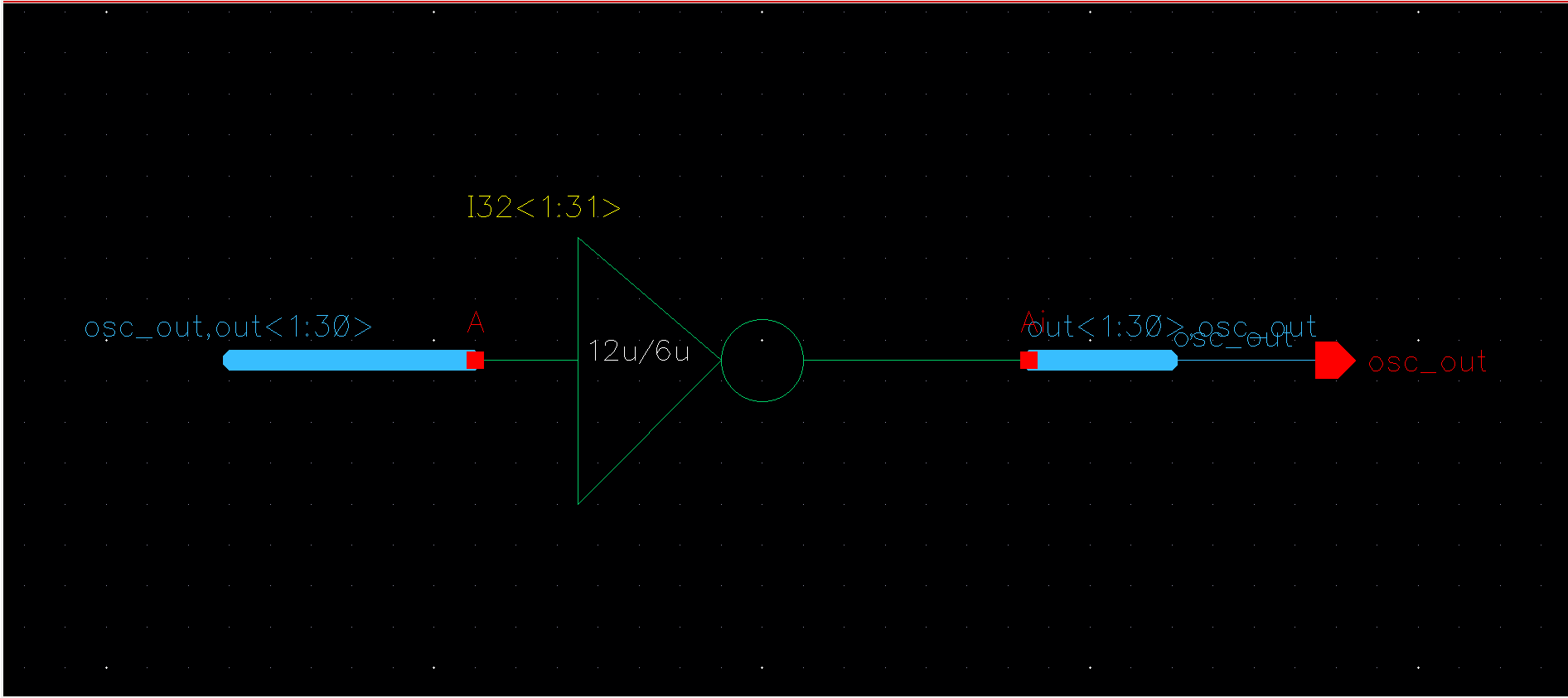
Ring oscillator of 31 invertersSymbol 
lab7/prelab/schematic_ringosc.PNGlab7/prelab/simulation_schematic.PNG
LayoutExtracted
lab7/prelab/layout_ringosc.PNGlab7/prelab/extracted_ringosc.PNG
   
Schematic SimulationExtracted Simulation
lab7/prelab/sim_ring_osc.PNGlab7/prelab/sim_ring_osc_extracted.PNG
 
Schematic ExtractedLVS
lab7/prelab/schematic_sim_boxthing.PNGlab7/prelab/extracted_sim_boxthing.PNGlab7/prelab/LVS.PNG


Lab:
 
 -Equivalent, more concise, schematic by instantiating an inverter and naming the inverter using an arrayed name (I0<3:0>)

Inverter Schematic (of one)The more concise schematic (of 4 of them)Symbol (of 4 of them)
lab7/lab7/INV/inverter_schematic.PNGlab7/lab7/INV/inverter_times4_schematic.PNGlab7/lab7/INV/inverter_times4_symbol.PNG
 
-Creating a simulation schematic like the one seen in the prompt
-
All four inverters' inputs are tied together to an input pulse source
 
SchematicSimulation
lab7/lab7/INV/invertlab7/lab7/INV/inverter_times4_simulation_schematic.PNGer_times4_symbol.PNGlab7/lab7/INV/inverter_times4_simulation_waveform.PNG
   
- The time delay will increase as the capacative load increases. If the capacitor is large, the amount of chargers that could be stored gets larger, which causes the voltage to take a longer time to rise and fall.
 
-Creating schematics and symbols for an 8-bit input/output array of: NAND, NOR, AND, inverter, and OR gates.

 
8-Bit NAND Gate:
NAND Schematic8-Bit NAND SchematicSymbol
lab7/lab7/NAND/NAND_SCHEMATIC.PNGlab7/lab7/NAND/NAND_SCHEMATIC_8.PNGlab7/lab7/NAND/NAND_SYMBOL_8.PNG
     
8-Bit NOR Gate:
NOR Schematic8-Bit NOR SchematicSymbol
lab7/lab7/NOR/NOR_SCHEMATIC.PNGlab7/lab7/NOR/NOR_SCHEMATIC_8.PNGlab7/lab7/NOR/NOR_SYMBOL_8.PNG
 
8-Bit AND Gate:
AND Schematic8-Bit AND SchematicSymbol
lab7/lab7/AND/1_BIT_AND_SCHEMATIC.PNGlab7/lab7/AND/8_bit_AND-SCHEMATIC.PNGlab7/lab7/AND/8_bit_AND_SYMBOL.PNG
   
8-Bit Inverter Gate:
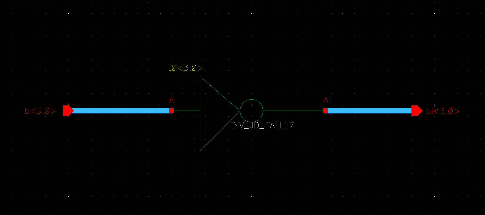
AND Schematic8-Bit Inverter SchematicSymbol
lab7/lab7/INV/8bit/1%20BIT%20INVERTER%20SCHEMATIC.PNGlab7/lab7/INV/8bit/INVERTER_8_SCHEMATIC.PNGlab7/lab7/INV/8bit/INVERTER_8_SYMBOL.PNG
 
8-Bit OR Gate:
 OR Schematic8-Bit OR SchematicSymbol
lab7/lab7/OR/OR_SCHEMATIC.PNGlab7/lab7/OR/OR%20SCHEMATIC%208.PNGlab7/lab7/OR/OR%20Symbol.PNG
     
-Me providing a few simulation examples using these gates.
Gate Simulation Schematic
lab7/lab7/sim_gates_lab7/schematic_sim_gates_lab7.PNG
   
NOR GATElab7/lab7/sim_gates_lab7/NOR_sim_gates_lab7.PNG
NAND
GATE
lab7/lab7/sim_gates_lab7/NAND_sim_gates_lab7.PNG
AND
GATE
lab7/lab7/sim_gates_lab7/AND_sim_gates_lab7.PNG
Inverter
GATE
lab7/lab7/sim_gates_lab7/INVERTER_sim_gates_lab7.PNG
OR
GATE
lab7/lab7/sim_gates_lab7/OR_sim_gates_lab7.PNG
 
 -Schematic of a 2-to-1 DEMUX/MUX (and the symbol)
SchematicSymbol
lab7/lab7/MUX/2%20-%201%20Mux/2-1-Mux_schematic.PNGlab7/lab7/MUX/2%20-%201%20Mux/2-1-Mux_symbol.PNG
 
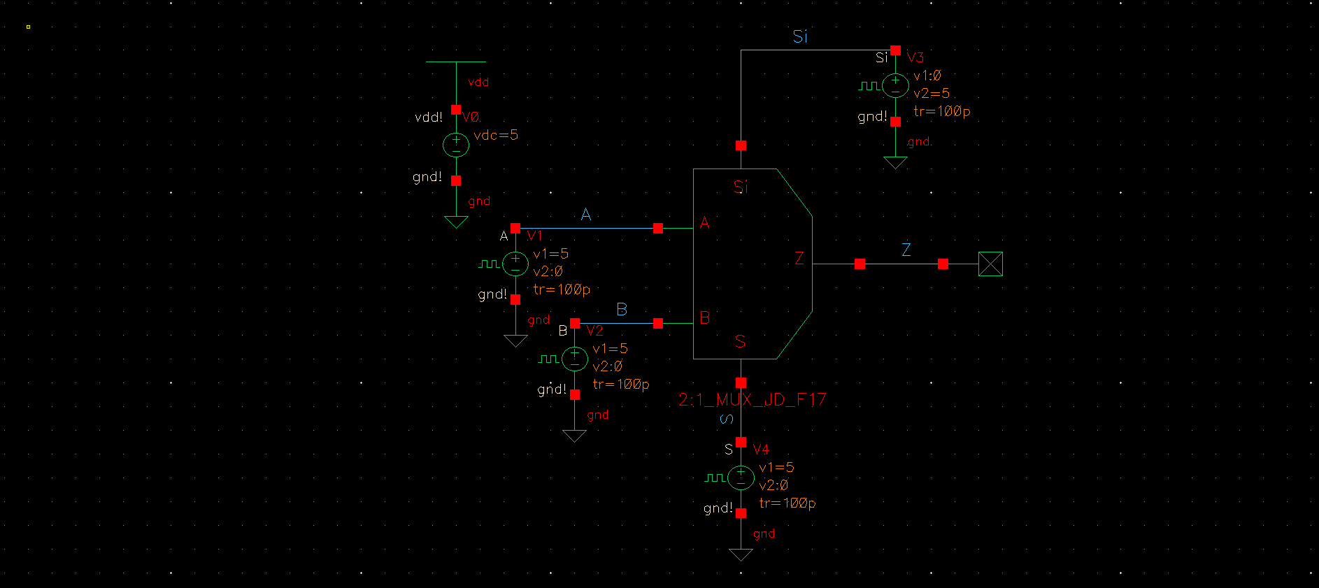
Schematic to simulateSimulation
lab7/lab7/MUX/2%20-%201%20Mux/mux%20sim%20schematic.PNGlab7/lab7/MUX/2%20-%201%20Mux/2-1-SIMULATION.PNG
 
-Including an inverter in the design, so the cell only needs one select input, S (the complement, Si, is generated using an inverter).
 
Schematic with the included inverterSymbol with one select input, S
lab7/lab7/MUX/2%20-%201%20MUX%20w-%20Inverter/21_MUX__WITH_INVERTER_SCHEMATIC.PNGlab7/lab7/MUX/2%20-%201%20MUX%20w-%20Inverter/21_MUX__WITH_INVERTER_SYMBOL.PNGlab7/lab7/MUX/2%20-%201%20MUX%20w-%20Inverter/21_MUX__WITH_INVERTER_SYMBOL.PNG
Simulation SchematicSimulation Results
lab7/lab7/MUX/2%20-%201%20MUX%20w-%20Inverter/mux%20inverter%20sim%20schematic.PNGlab7/lab7/MUX/2%20-%201%20MUX%20w-%20Inverter/21_MUX__WITH_INVERTER_SIMULATION.PNG
 
The inverter has no effect on the results, so it does not matter if its attached or not.
 
2-to-1 Demux SchematicSimulation
lab7/lab7/MUX/Demux/21_DEMUX_SCHEMATIC.PNGlab7/lab7/MUX/Demux/21_DEMUX_SIMULATION.PNG
 
-An 8-bit wide word 2-to-1 DEMUX/MUX schematic and symbol
SchematicSymbol
lab7/lab7/MUX/8_BIT_2_TO_1_MUX_SCHEMATIC.PNGlab7/lab7/MUX/8_BIT_2_TO_1_MUX_SYMBOL.PNG
Schematic SimulationSimulation Results
lab7/lab7/MUX/8_BIT_2_TO_1_MUX_SCHEMATIC_SIM.PNGlab7/lab7/MUX/8_BIT_2_TO_1_MUX_SIMULATION.PNG

-
A schematic of the full-adder seen in Fig. 12.20 using 6u/0.6u devices (both PMOS and NMOS)
SchematicSymbolLayoutExtracted
lab7/lab7/Full%20Adder/1-bit-fooladdahh/FULL_ADDER_SCHEMATIC.PNGlab7/lab7/Full%20Adder/1-bit-fooladdahh/FULL_ADDER_SYMBOL.PNGlab7/lab7/Full%20Adder/1-bit-fooladdahh/FULL_ADDER_LAYOUT.PNGlab7/lab7/Full%20Adder/1-bit-fooladdahh/FULL_ADDER_EXTRACTED.PNG
   
Simulation SchematicResults
lab7/lab7/Full%20Adder/1-bit-fooladdahh/FULL_ADDER_SIMULATION_SCHEMATIC.PNGlab7/lab7/Full%20Adder/1-bit-fooladdahh/FULL_ADDER_EXTRACTED_SIMULATION.PNG
 
LVSDRC
lab7/lab7/Full%20Adder/1-bit-fooladdahh/FULL_ADDER_LVS.PNGlab7/lab7/Full%20Adder/1-bit-fooladdahh/FULL_ADDER_DRC.PNG

-Lay out this 8-bit adder cell

SchematicSymbol
lab7/lab7/Full%20Adder/8-bit-fulladdahhh/8_BIT_FULLADDAH_SCHEMATIC.PNGlab7/lab7/Full%20Adder/8-bit-fulladdahhh/8_BIT_FULLADDAH_SYMBOL.PNG
LayoutExtracted
lab7/lab7/Full%20Adder/8-bit-fulladdahhh/8_BIT_FULLADDAH_LAYOUT.PNGlab7/lab7/Full%20Adder/8-bit-fulladdahhh/8_bitFULLADDEREXTACTEDF.PNG
   
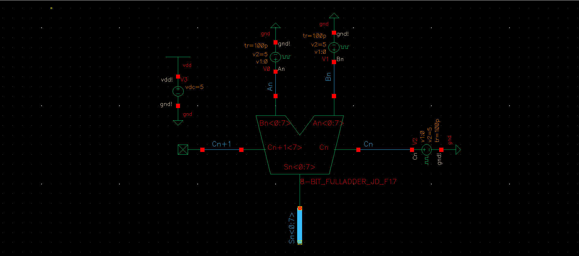
Schematic simulationResults
lab7/lab7/Full%20Adder/8-bit-fulladdahhh/8_bitFULLADDERSIMSCHEMATIC.PNG lab7/lab7/Full%20Adder/8-bit-fulladdahhh/8_BIT_FULLADDAH_SIMULATION_SCHEMATIC.PNG
 
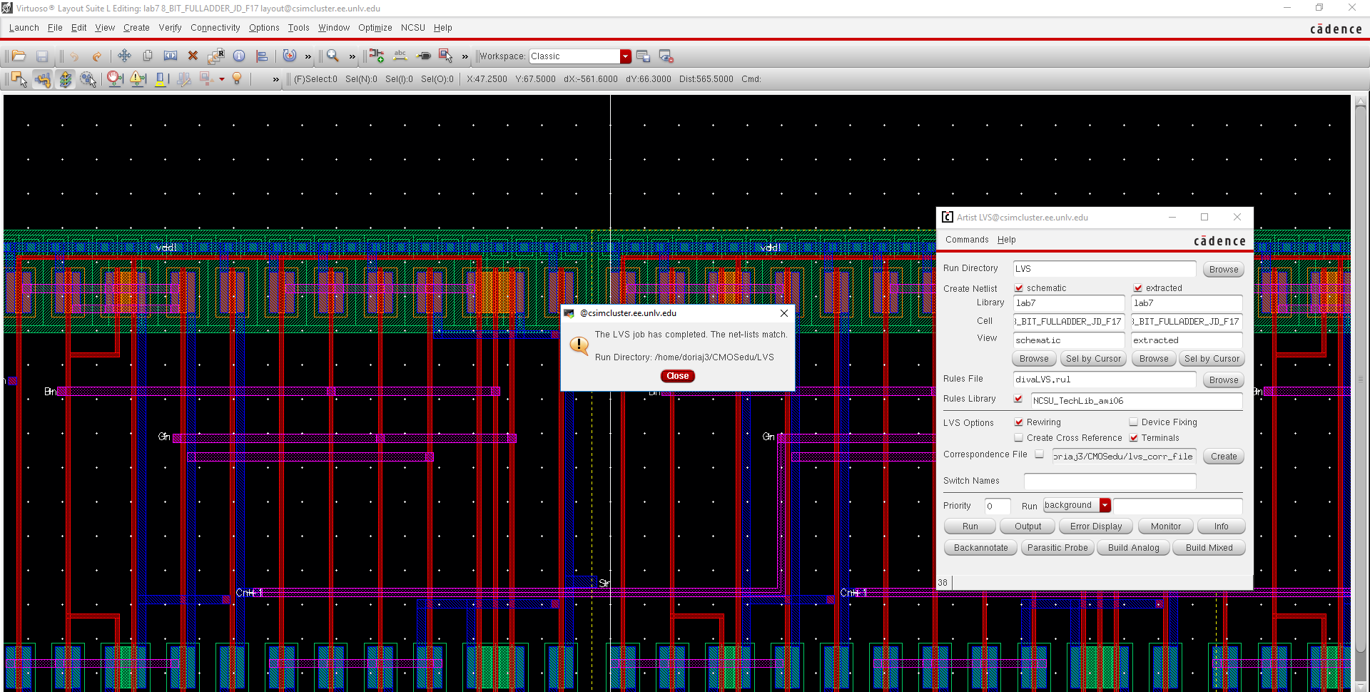
LVS:
lab7/lab7/Full%20Adder/8-bit-fulladdahhh/8-BIT_ADDER_LVS.PNG
DRC:
lab7/lab7/Full%20Adder/8-bit-fulladdahhh/8_BIT_FULLADDAH_LAYOUT_DRC.PNG

-Backing up files
lab7/backup.PNG


Lab 7 Files Download
Return to not my lab 7