Lab 6 - EE 421L
Jeeno Doria
doriaj3@unlv.nevada.edu
10/23/2017
Lab
description: Go through tutorial 4 and use the skills acquired to design and layout a full adder.
PreLab:
- Me going through Cadence Tutorial 4..
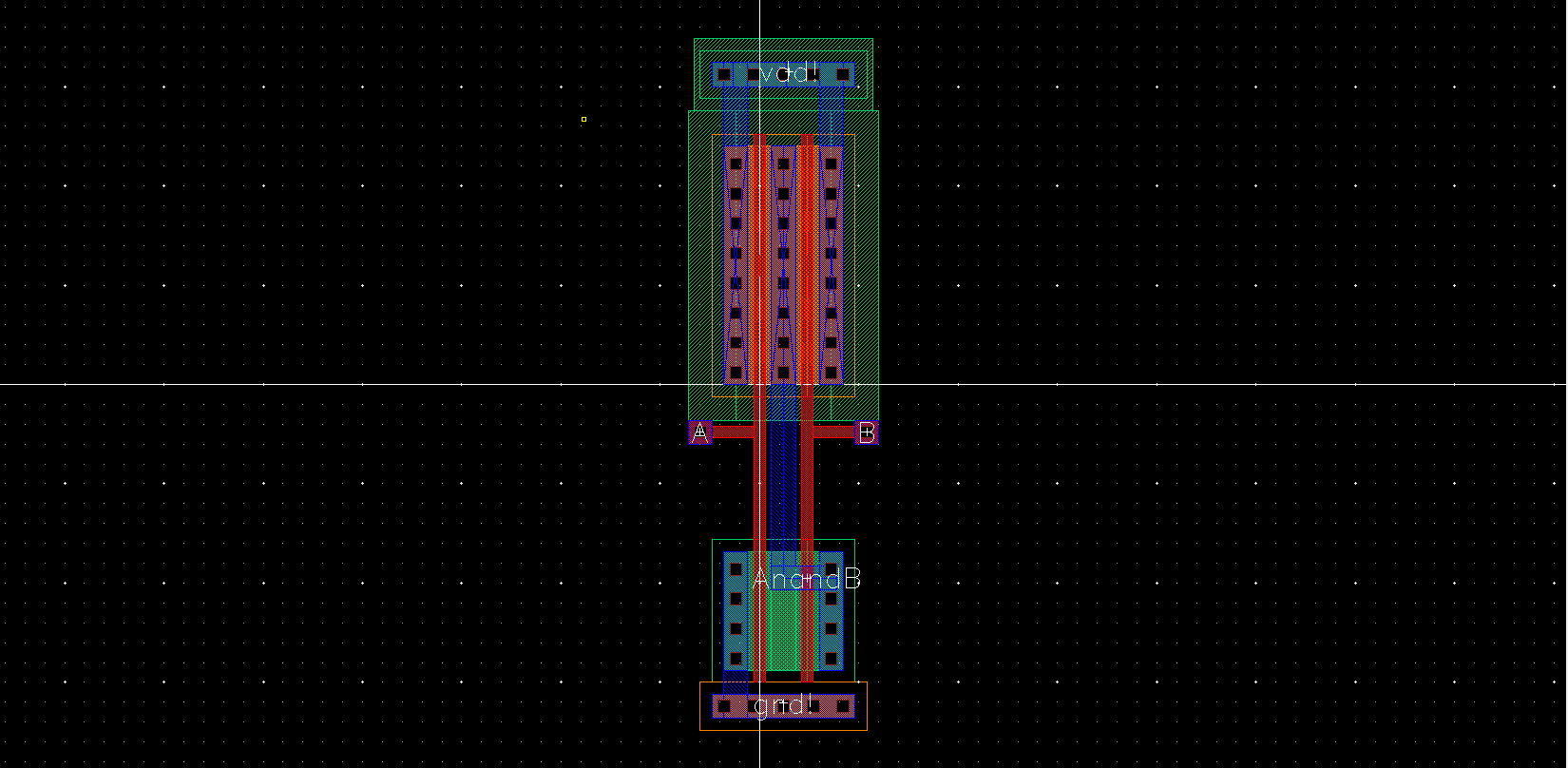
-Schematic of a NAND gate
| NAND Schematic | NAND Layout | Simulation Schematic |
 | 
| 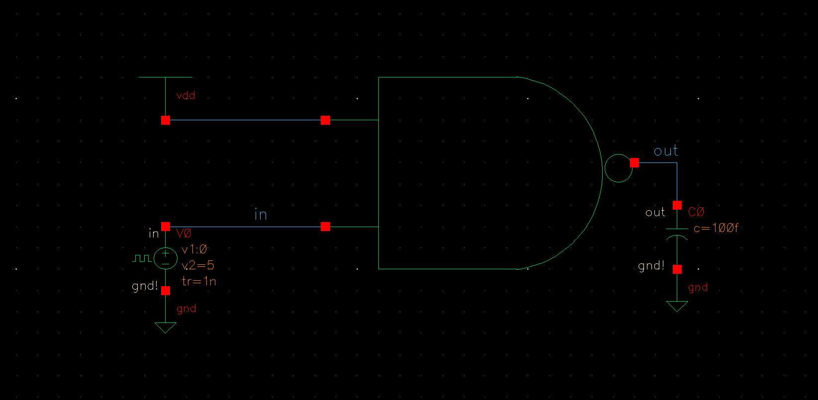 |
-Wave Form
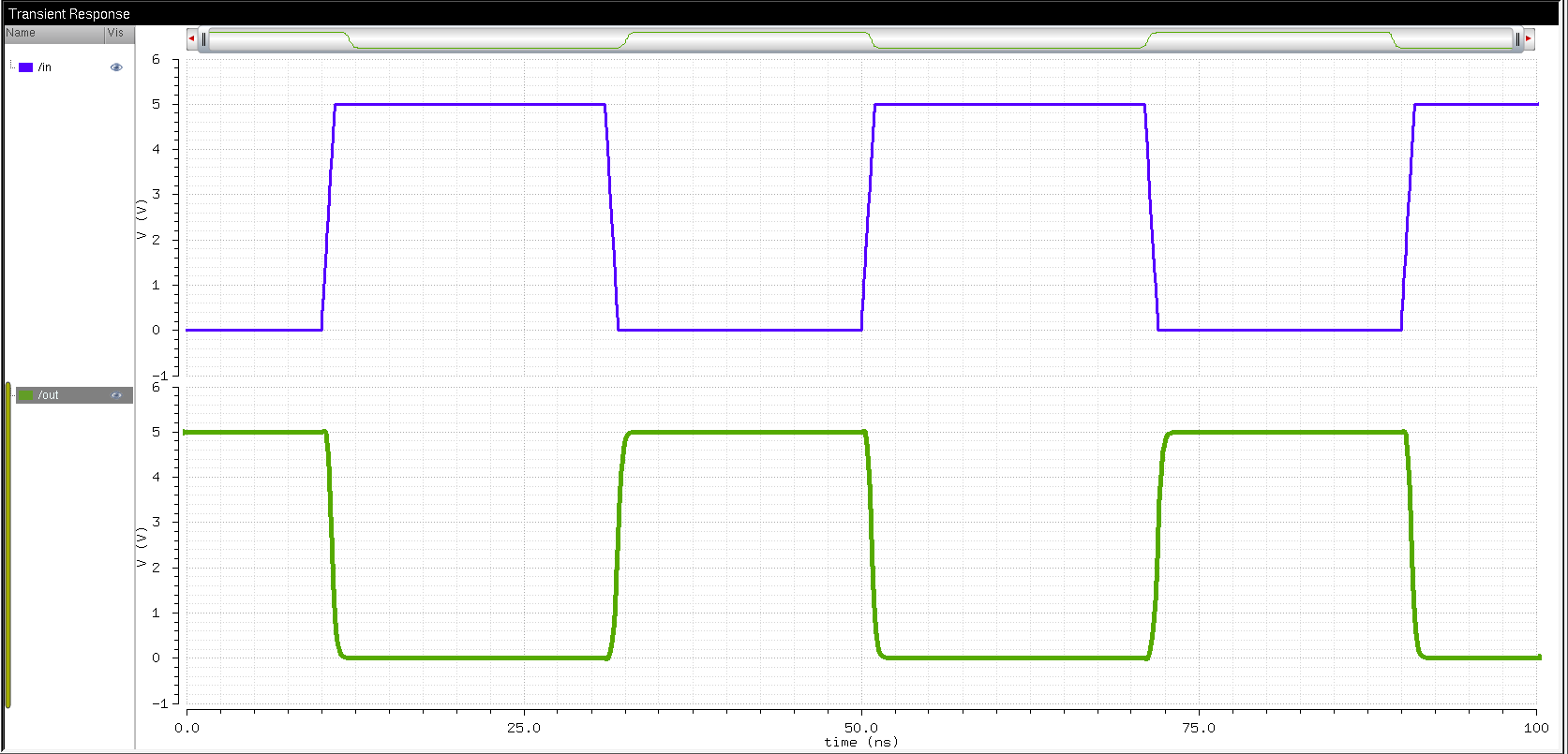
| LVS |
 |
Lab:
- Draft
the schematics of a 2-input NAND gate (Fig. 12.1), and a 2-input XOR
gate (Fig. 12.18) using 6u/0.6u MOSFETs (both NMOS and PMOS)
- Create layout and symbol views for these gates showing that the cells DRC and LVS without errors
| NAND Schematic | NAND Symbol |
 |  |
| NAND Layout | NAND Extracted |
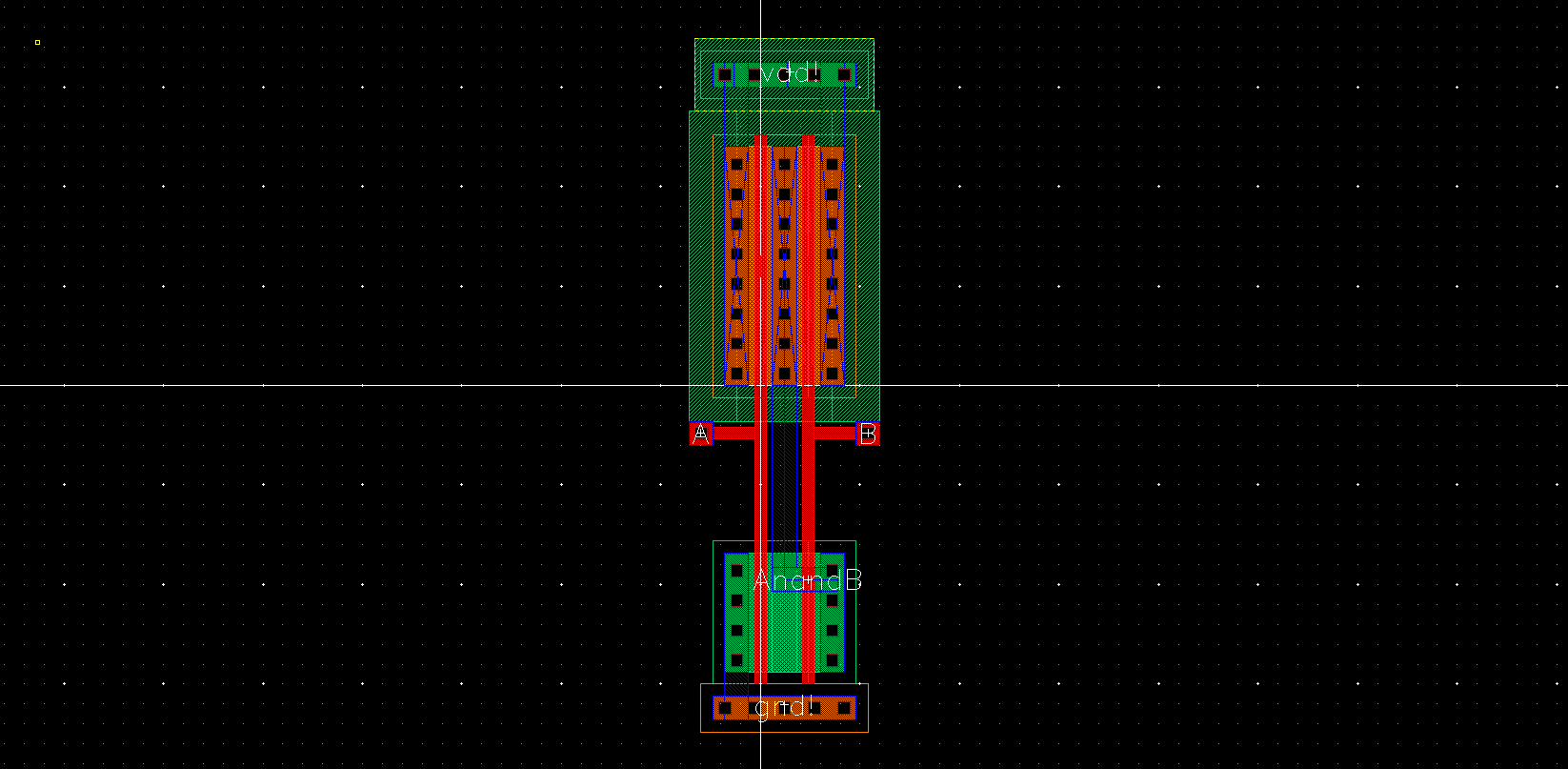 |  |
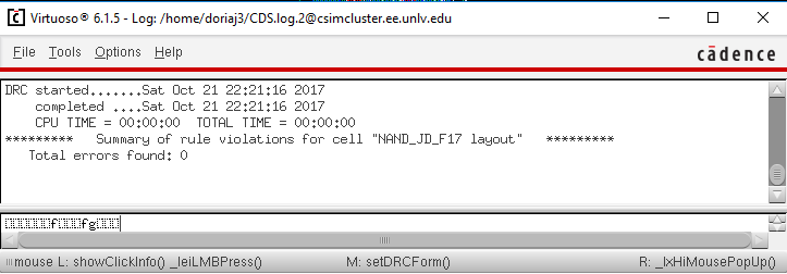
-DRC
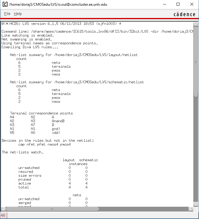
-LVS
| XOR Schematic | XOR Symbol |
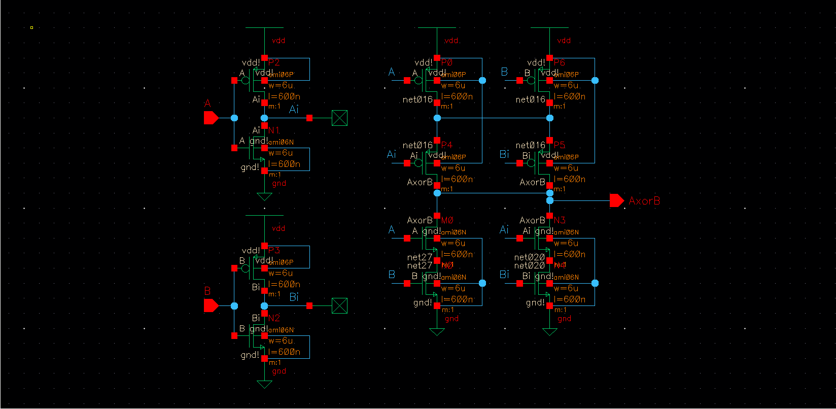 | 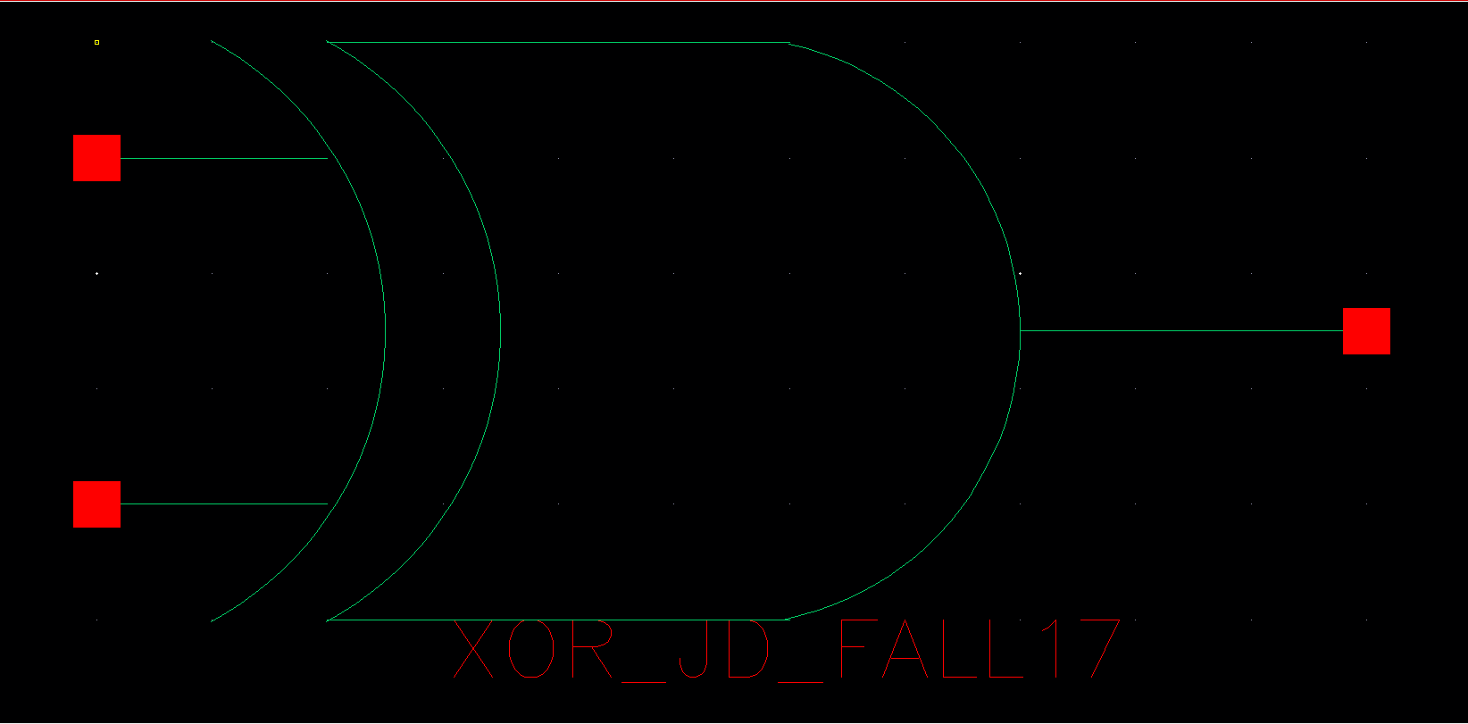 |
| XOR Layout | XOR Extracted |
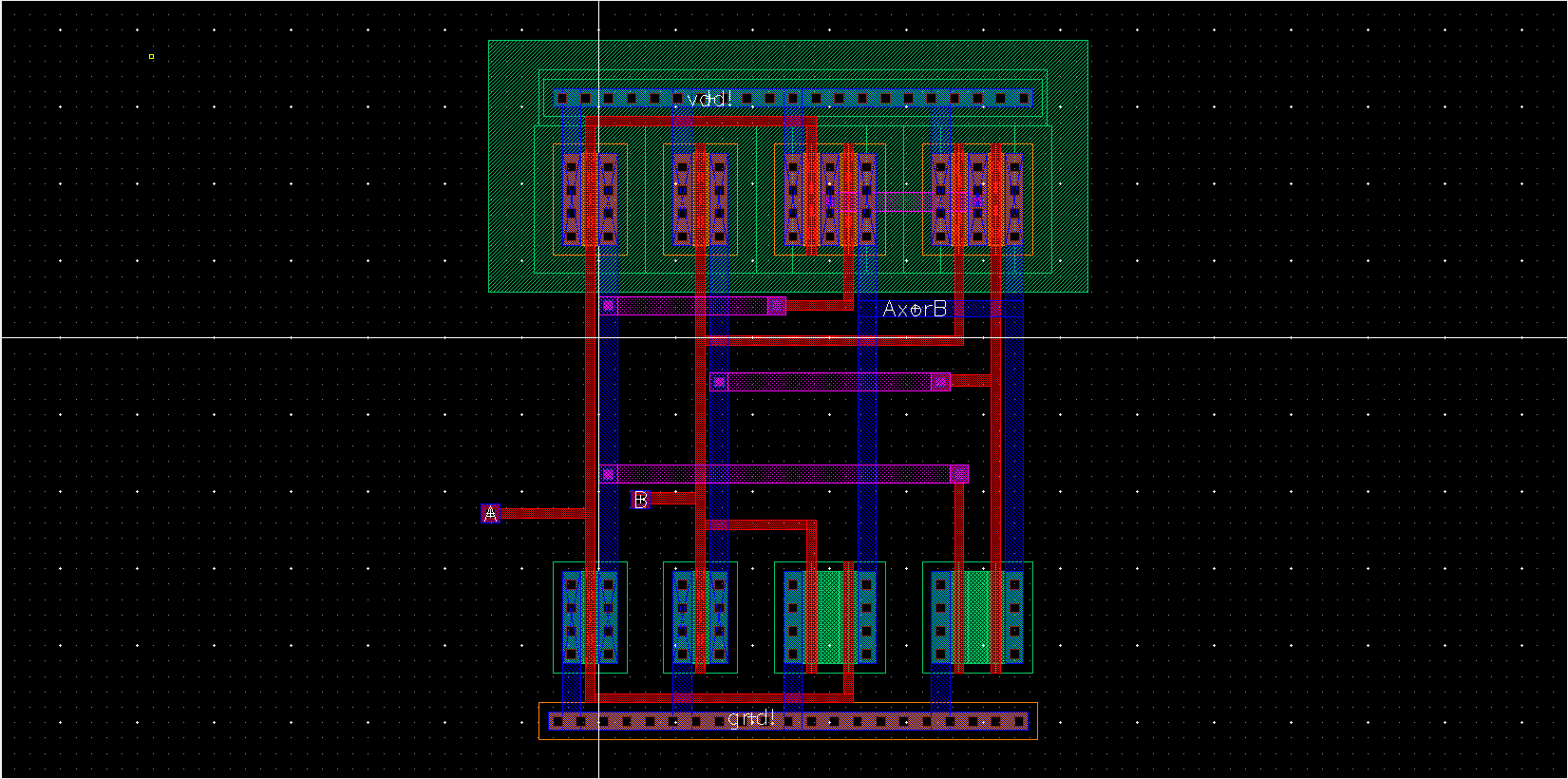 | 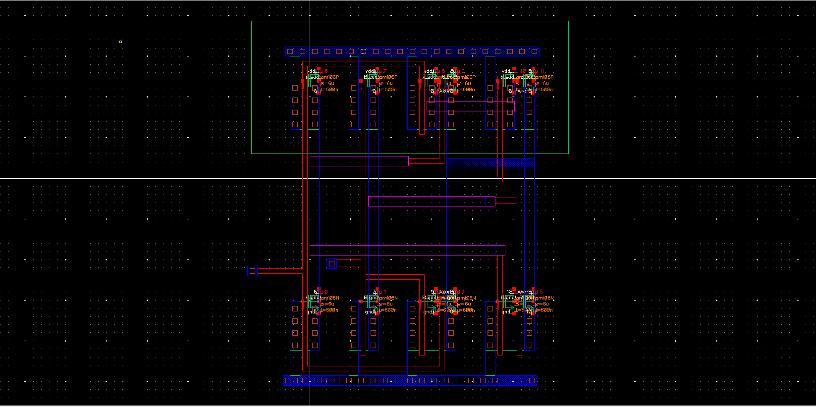 |
-DRC
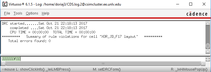
-LVS
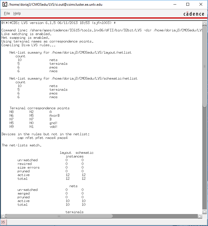
- Using Spectre to simulate the logical operation of the gates for all 4 possible inputs (00, 01, 10, and 11)
| Schematic | Wave Form |
 | 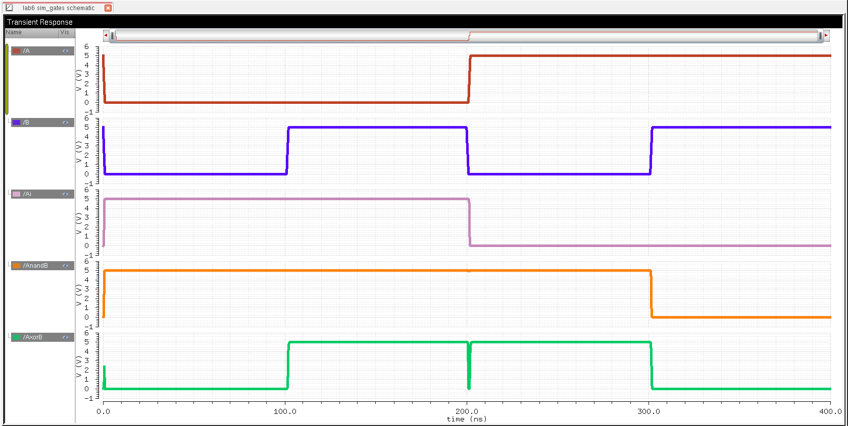 |
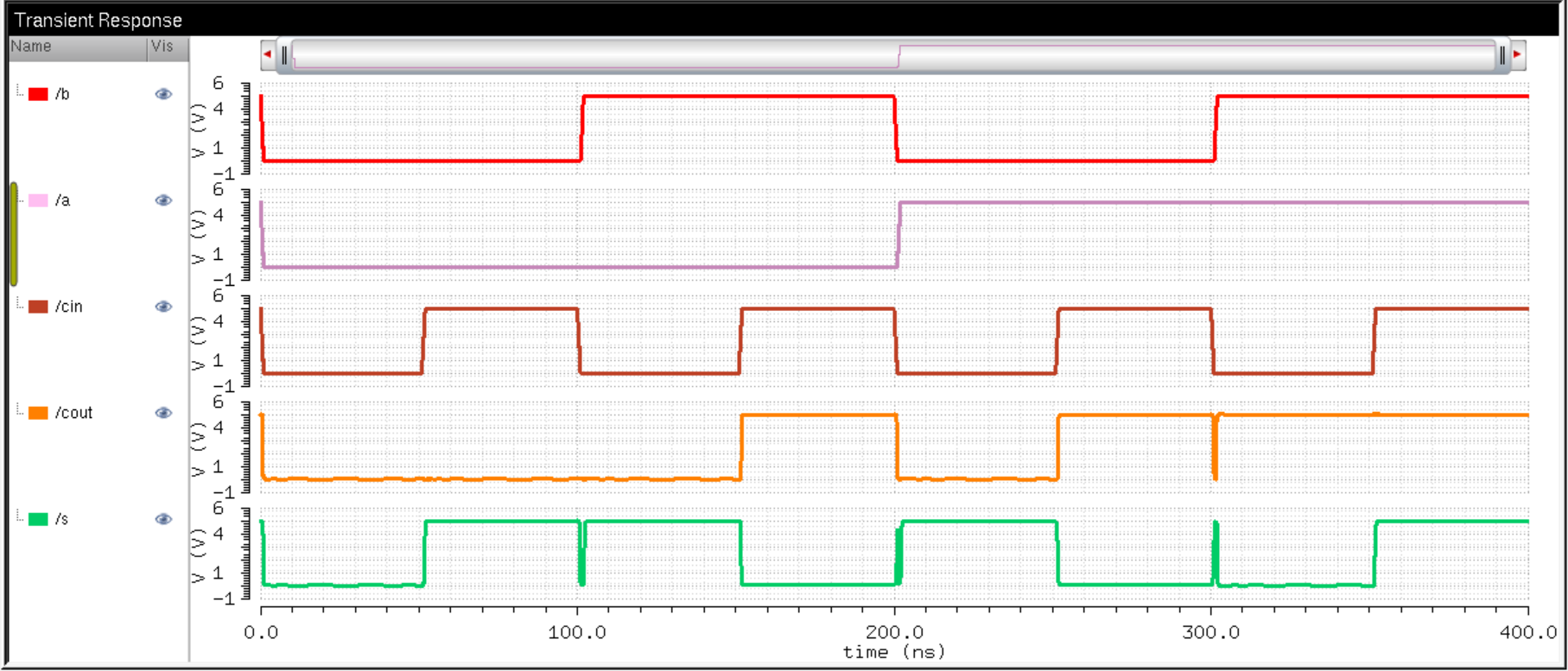
- There
are glitches when the voltage drops on input a and rises on b (vise
versa) at same time. The rising and falling edge of both inputs
are very close at around 200ns, which causes the cout to fall and rise
at a very short time.
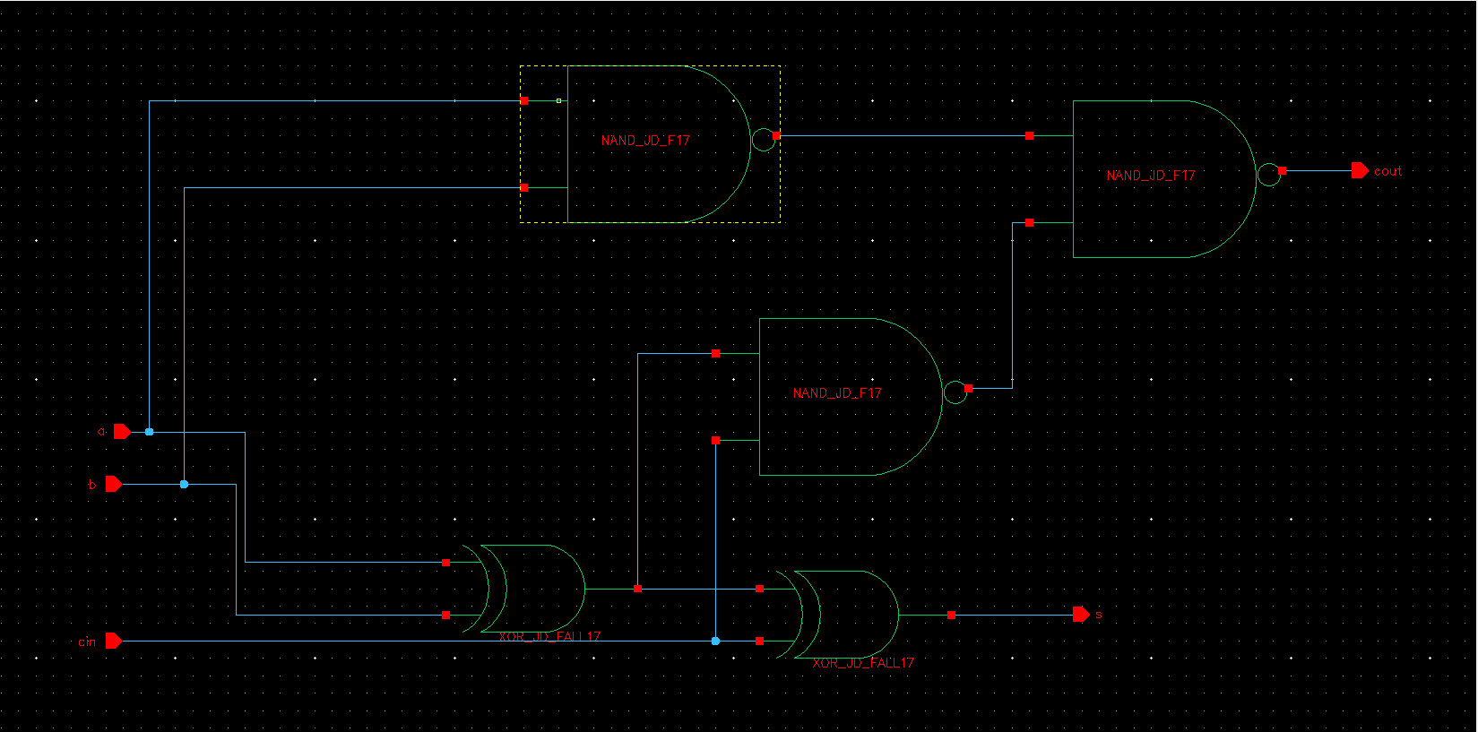
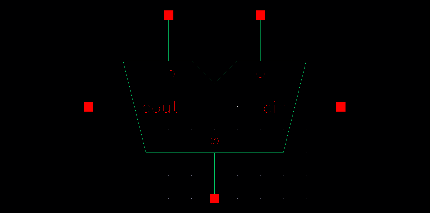
-Full Adder
| Full Adder Schematic | Full Adder Layout | Full Adder Symbol |
 | 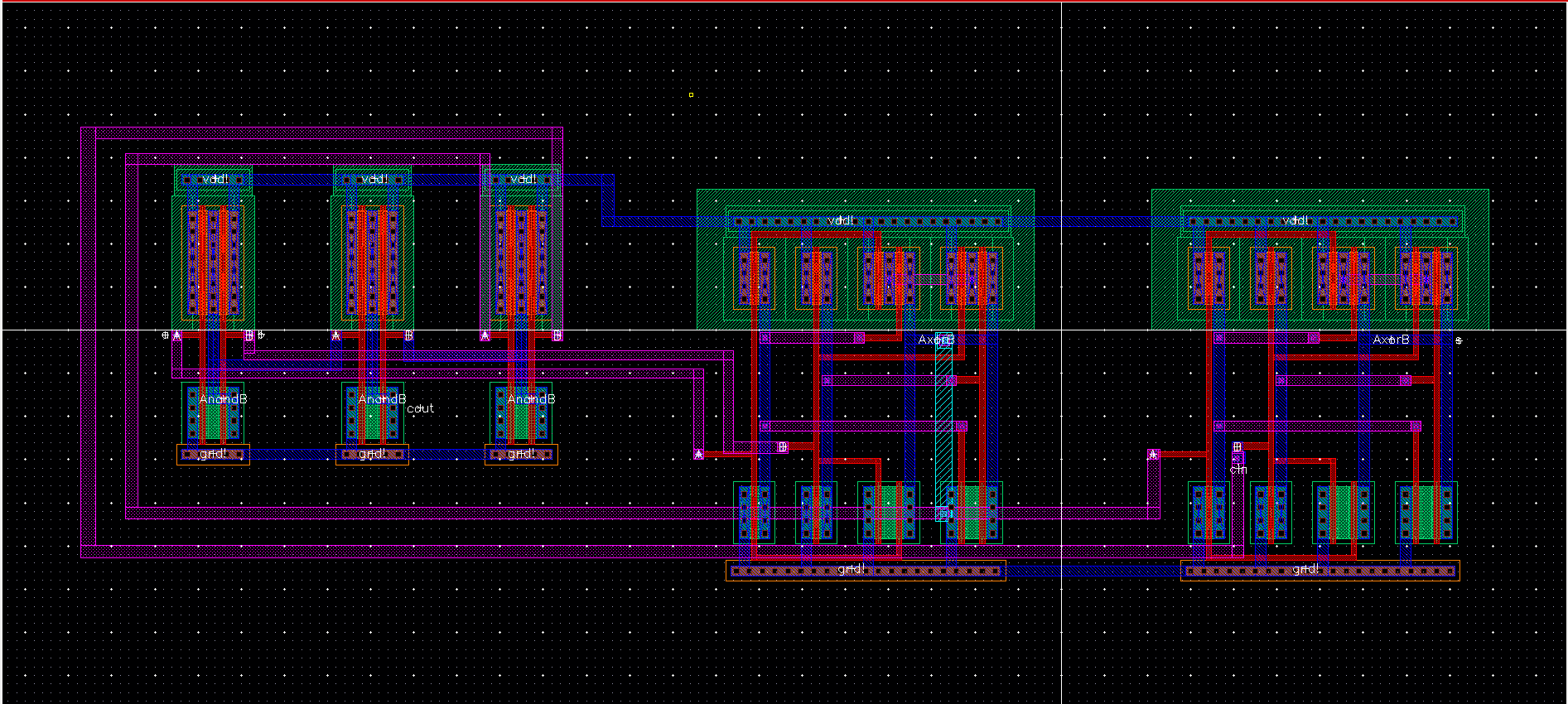 |  |
-DRC

-LVS
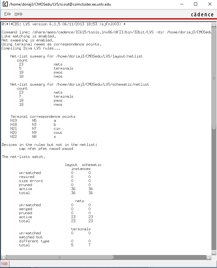
- Simulating with Spectre the operation of the full-adder using this symbol..
| Schematic | Wave Form |
 |  |
-Stuff backed up on google drive

Download Lab6.zip
Return to not lab 6