Lab 5 - EE 421L
Jeeno Doria
9/28/2017
doriaj3@unlv.nevada.edu
Lab
description: In this lab we will draft schematics, layouts, and symbols
for two inverters. These inverters will have the size of 12u/6u and
48u/24u.
Pre Lab:
- Back-up all of your work from the lab and the course.
- Go through Tutorial 3
-My work being backed up
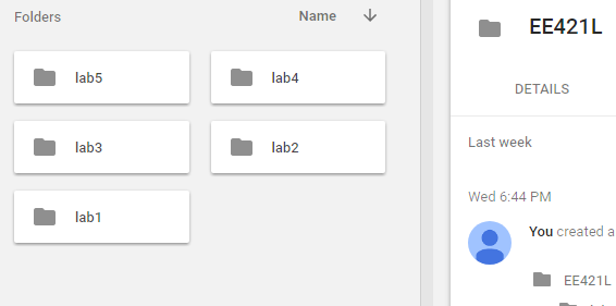
-Going through Tutorial 3
| LVS | Simulation |

| 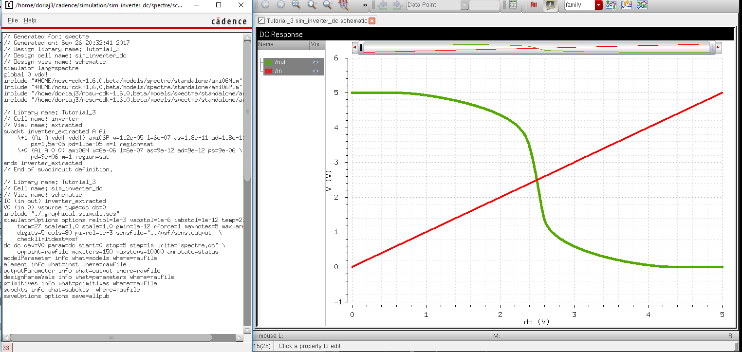 |
Lab:
I Basically did what was covered in Tutorial 3. To create a 48u/24u inverter, we have to adjust the multiplier to 4 in the schematic and layout. In the layout, minor adjustments were made after changing the multiplier since there are now 4 mosfets.
- Power (vdd!) is connected to the n-well using the ntap cell
- Ground (gnd!) is connected to the p-substrate using the ptap cell
- The schematics have two pins, e.g., A and Ai
- layouts having 4 pins: A, Ai, vdd!, and gnd!
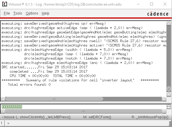
- Results showing that the extracted layouts and schematics LVSed correctly
| Extracted: | Layout DRC | LVS: 12u/6u |
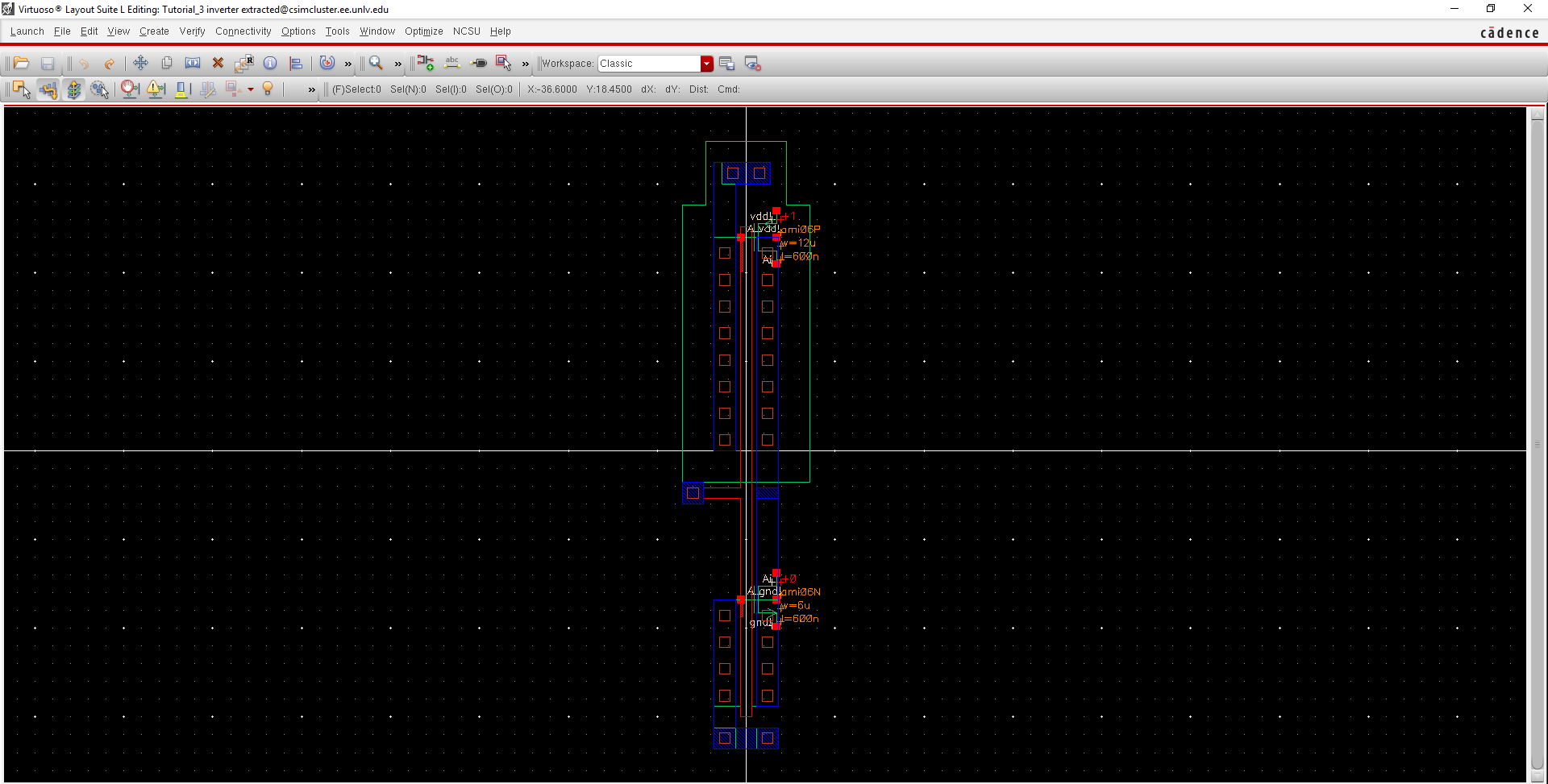 | 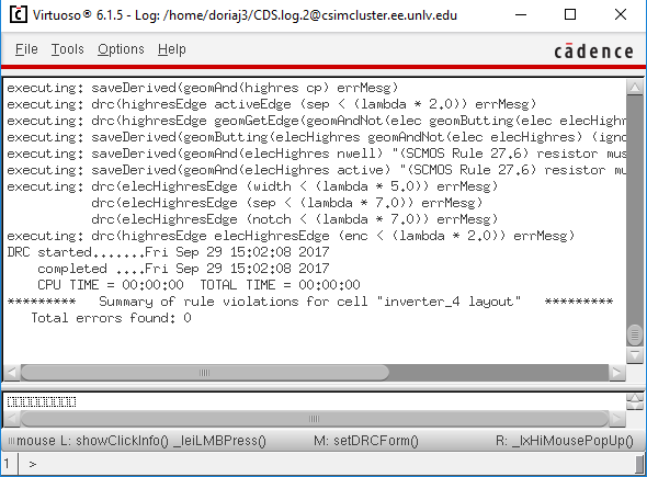 |  |
 | 
|  |
-Spectre Simulation
-switching simulator modes from Spectre to UltraSim

-UltraSim Simulation of an inverter with the size of 12u/6u. | Capacitor Load | Schematic | Simulation |
| 100f | 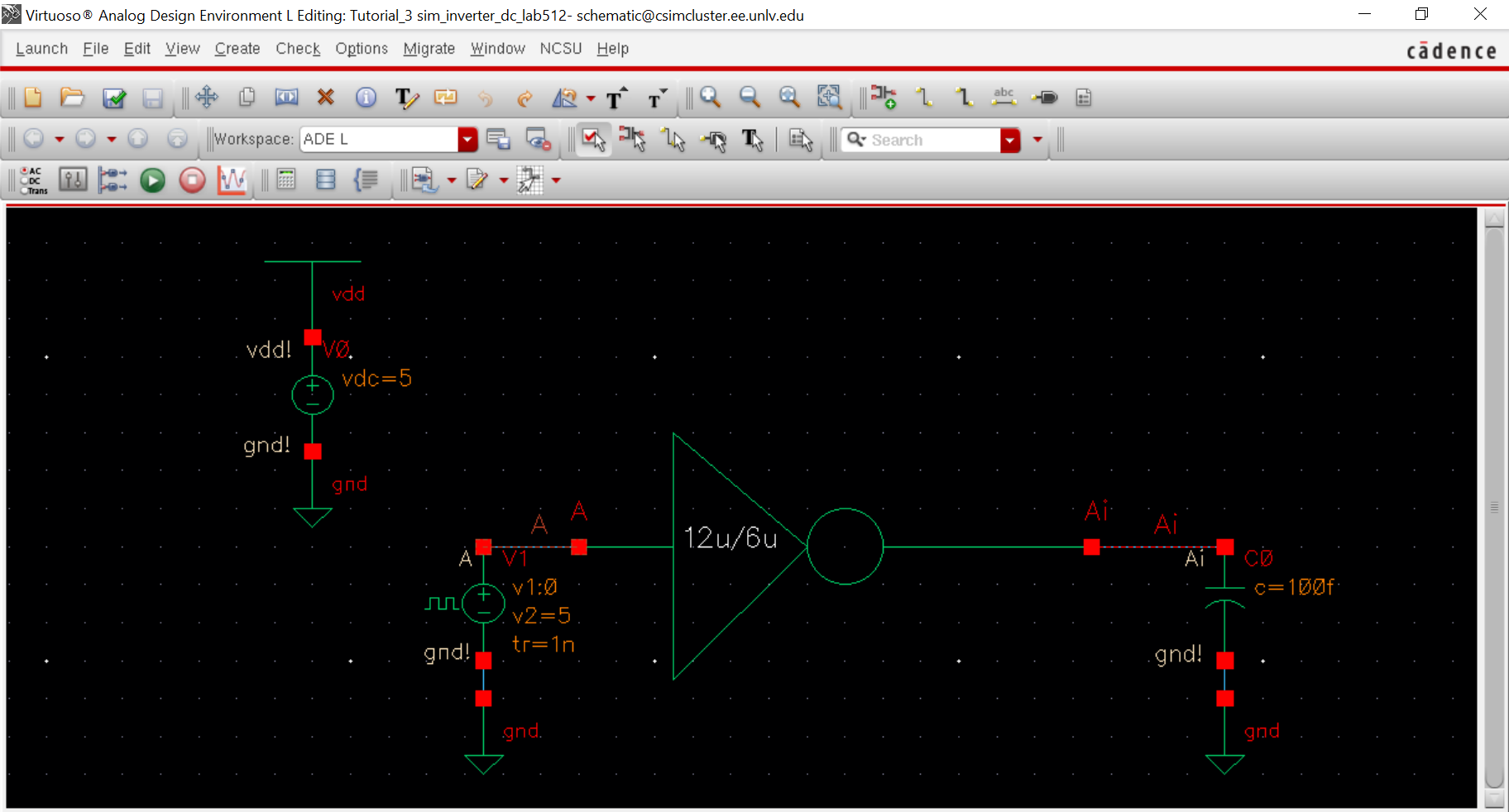 | 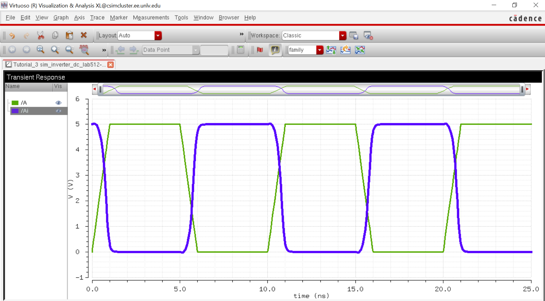
|
| 1p |  | 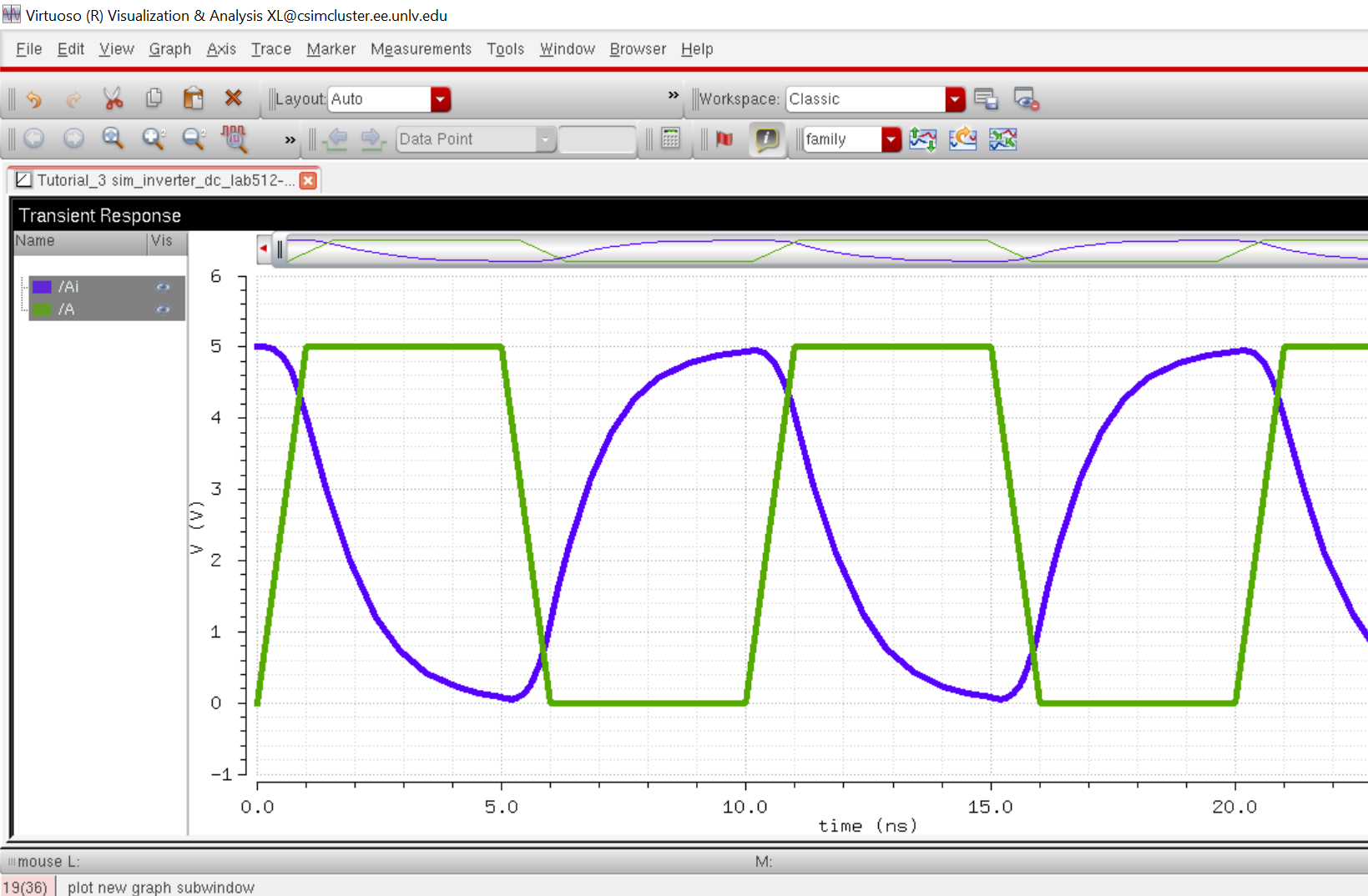 |
| 10p | 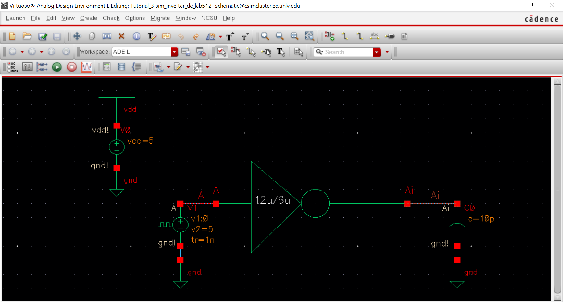 | 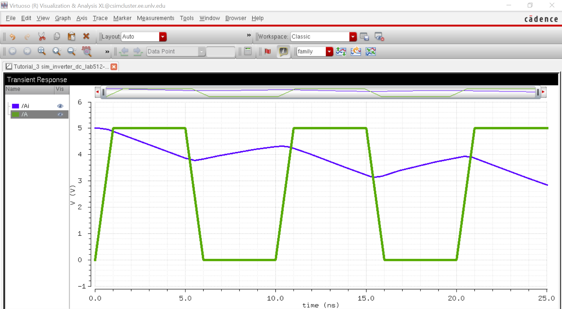 |
| 100p | 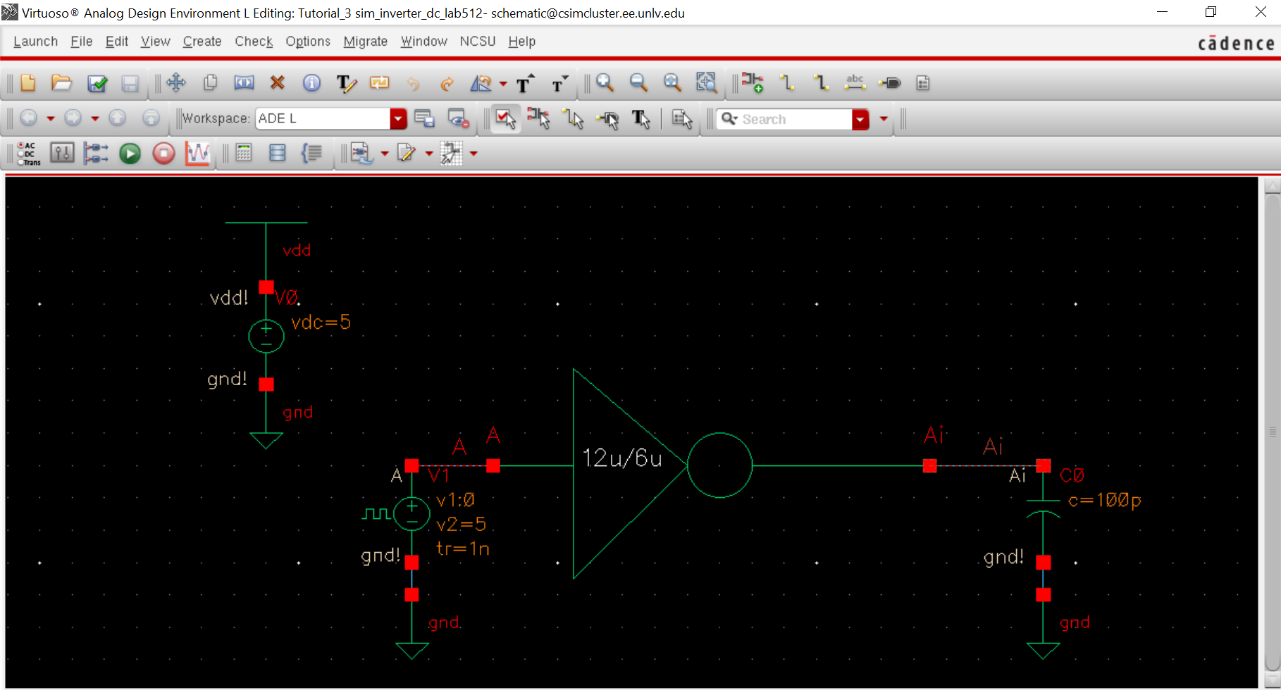 |  |
-By looking through the different simulations that differ in capcitave load, I came to the conclusion that the signal inverts slower as capacitance increases.
-UltraSim Simulation of an inverter with the size of 48u/24u.
| Capacitor Load | Schematic | Simulation |
| 100f | 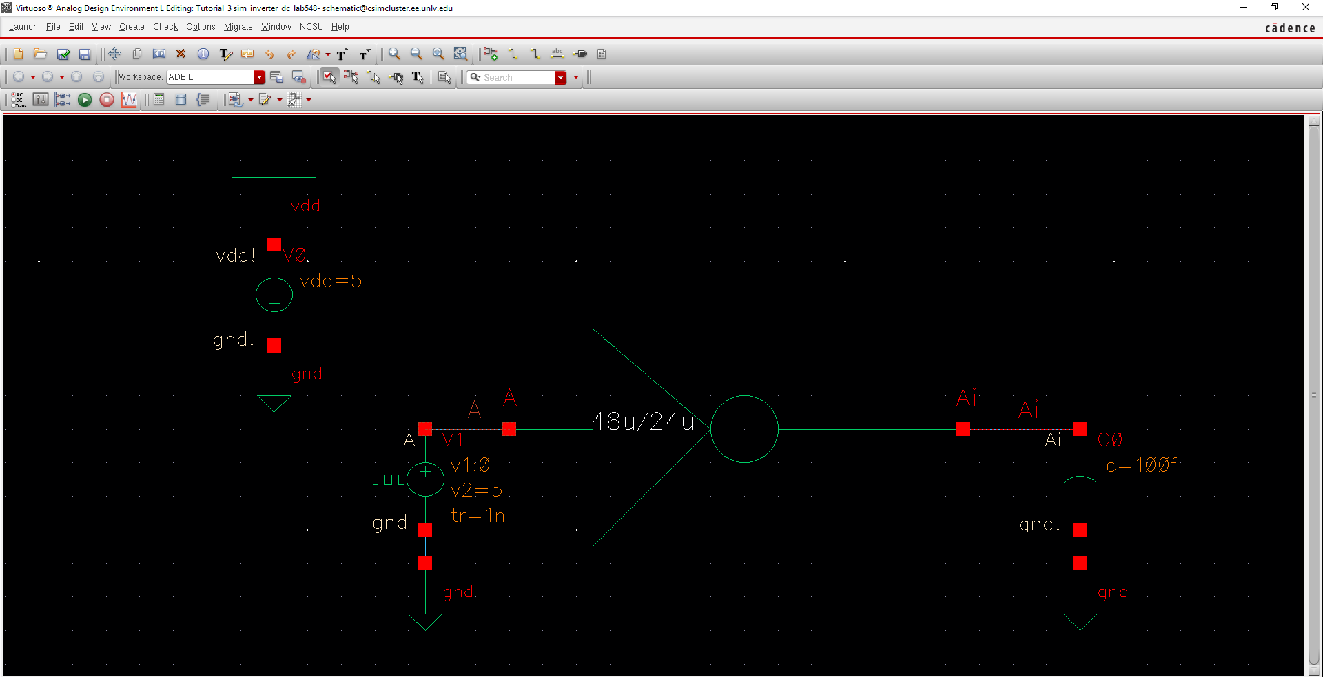 | 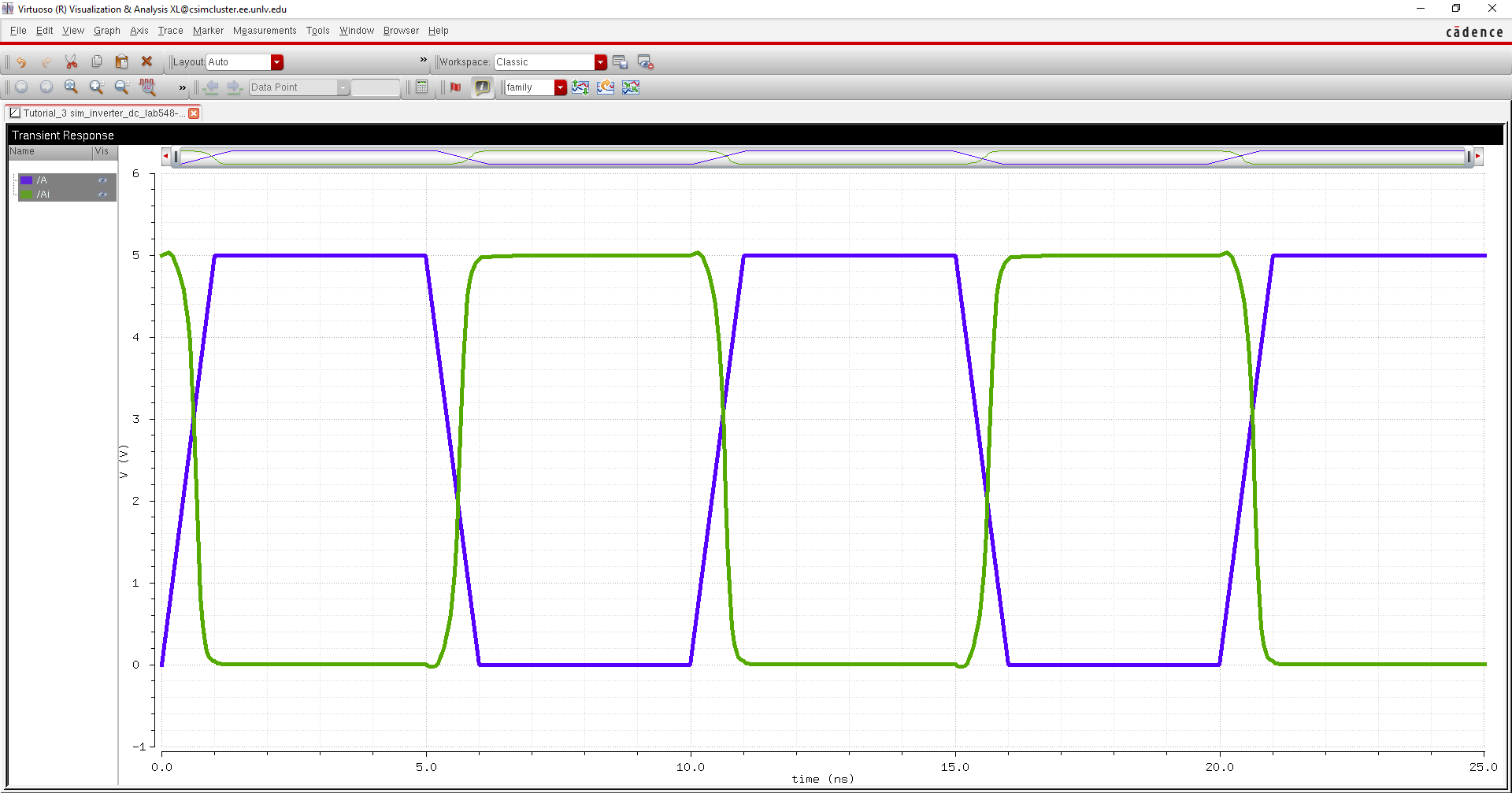 |
| 1p | 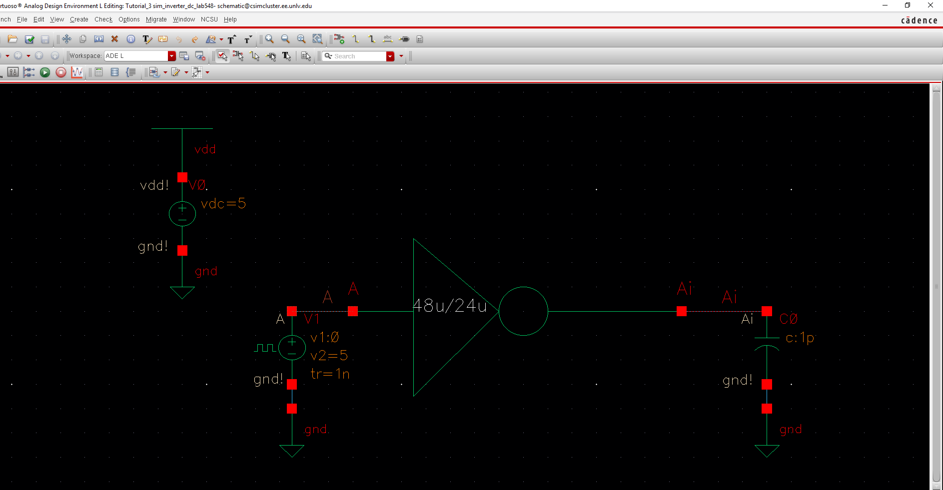 | 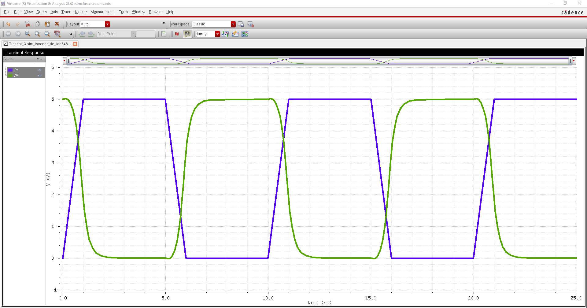 |
| 10p | 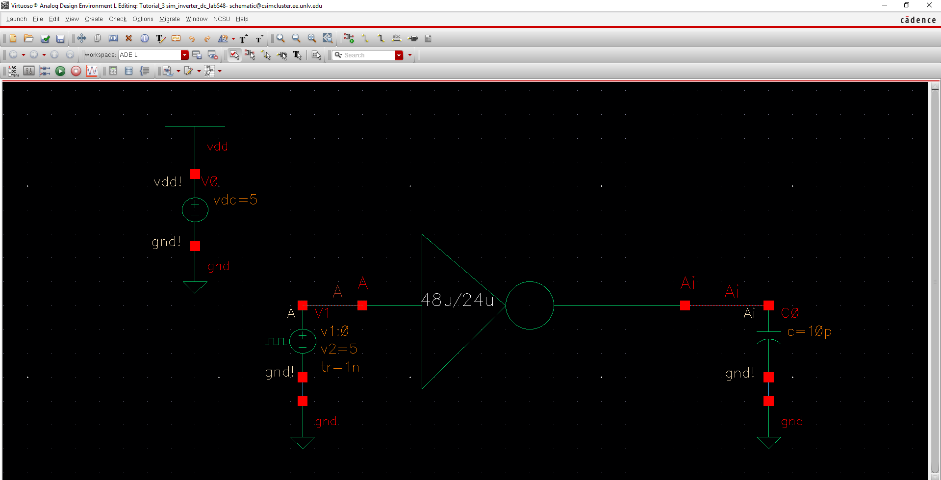 | 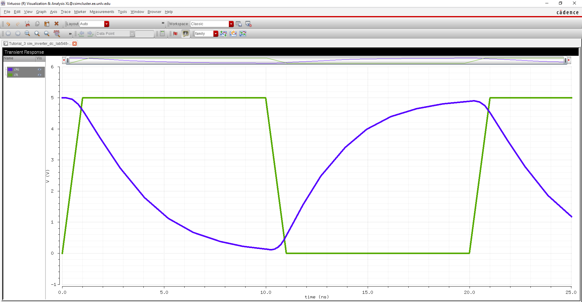 |
| 100p | 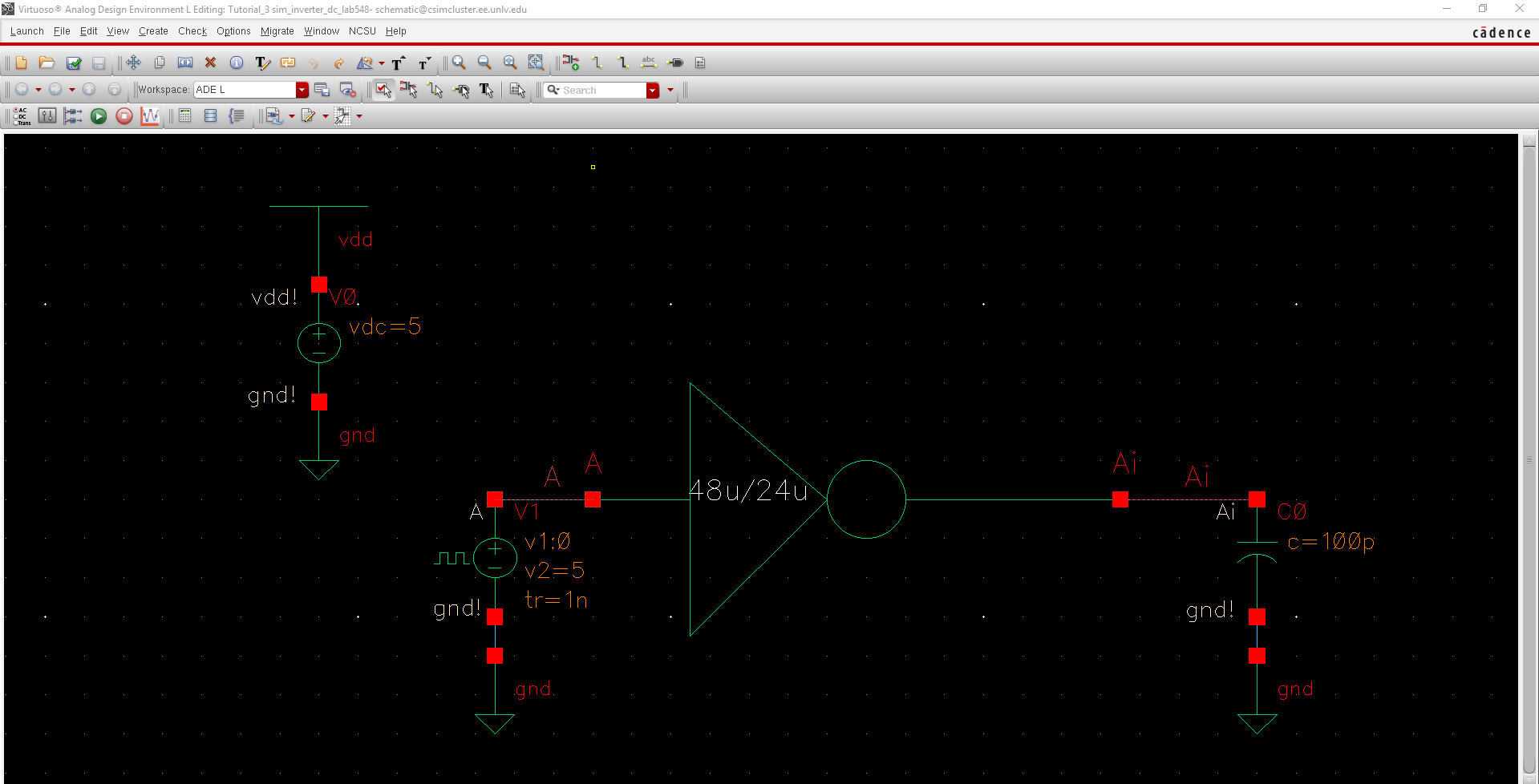 |  |
-It is the same circumstance as the set of simulations before, but it is inverting the signal more quickly.
Download Lab5 files
Return to not my lab 5