


Lab Project - EE 421L
The Inverter:
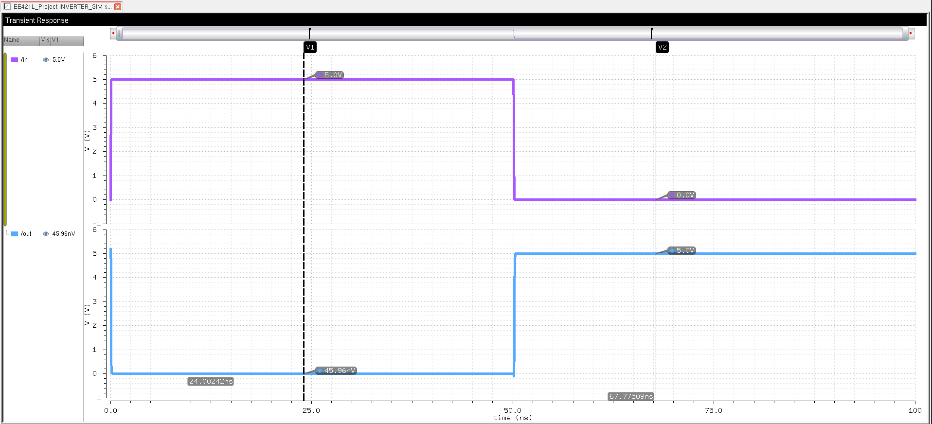
| Schematic | Schematic Simulation |
| |
| Layout | Waveform |
| |
| Extracted | LVS |
| |

The Xor:
| Schematic | Schematic Simulation |
 |  |
| Layout | Waveform |
 |  |
| Extracted | LVS |
 |  |

The Buffer:
| Schematic | Symbol |
 |  |
| Layout | Extracted |
 |  |
The Even Parity Checker:
- The inputs to my circuit are D0-D7, P and the output is check
- The output of the design, check, is buffered before connecting to a pad
- The parity input is "xor'd" to the even binary set of inputs to determine if the output is TRUE
- An even binary set of inputs include D0-D7 and the parity input
| Schematic | Symbol |
 |  |
| Layout | Extracted |
 |  |
| LVS | DRC |
 |  |
| Schematic Simulation | Waveform |
 |  |
| Extracted Simulation | Netlist Display |
 |  |