Project - ECE 421L
Design, Layout and Simulation of a Detector
Project Objective - design a circuit that takes a serial input and detects the sequence 101011Detector Operation
The detection of a serial input sequence 101011 is most easily done with a 6 bit serial-in, parallel-out shift register.
We
"detect" the input 101011 by using a 6 bit AND gate (or equivalent
circuit) fed either Q or Qbar from each register (Q when the bit is
expected to be '1' and Qbar when bit is expected to be '0' (Qbar =
'1')).
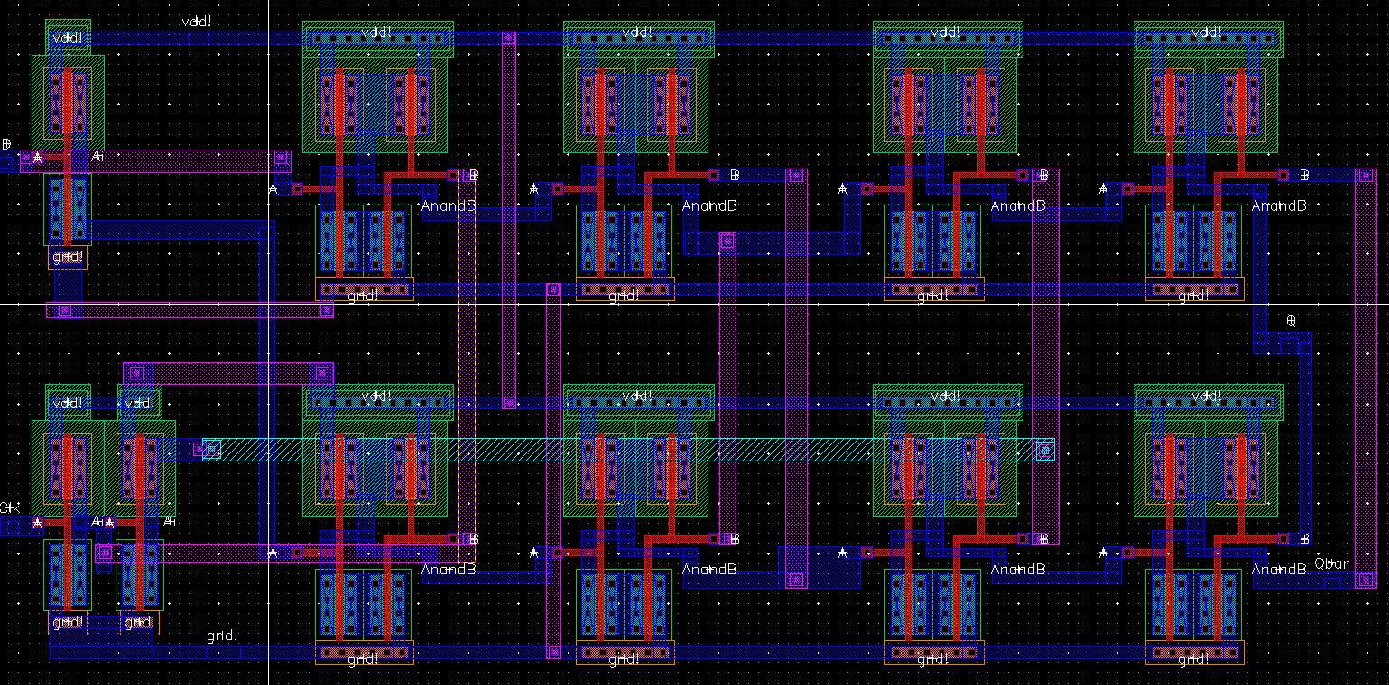
Rising Edge Triggered D-FF
This device will read a value (0 or 1) from input "D" on all rising edges of the signal "Clk" and will hold that value until the next rising edge "Clk" signal.
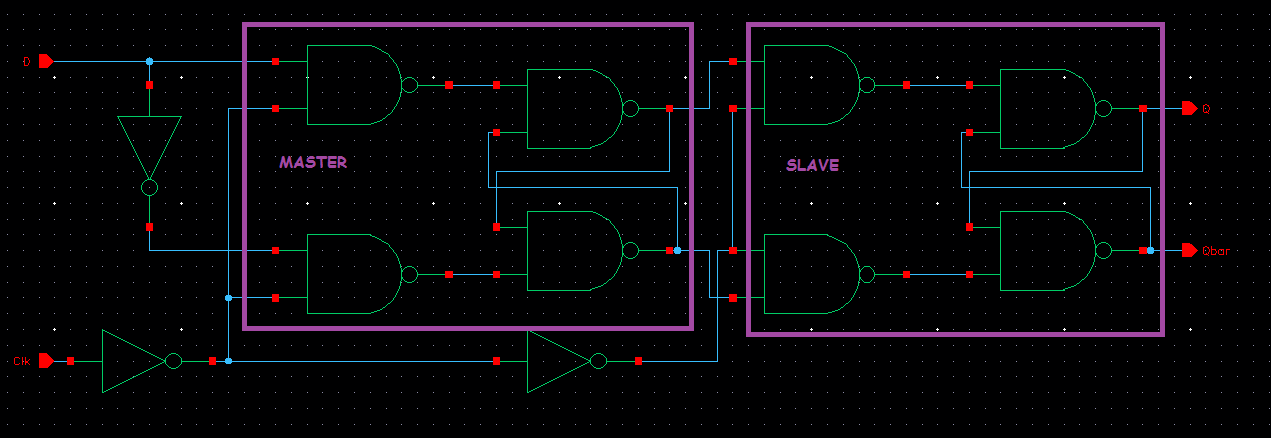
Rising Edge Triggered D-FF Schematic
The edge triggered D-FF was created by putting two D-latch
gates together in Master/Slave format. The left four AND2 gates represent
the Master D-latch, and the right four AND2 gates represent the Slave D-latch.
The Master D-latch see the "enable" signal when "Clk" is
low. This stores or "locks" the information in the Master D-latch
when going from low to high "Clk" signal.
During this transition from low to high "Clk", the Slave is now
accepting information that is being fed from the "locked" Master.
The Master D-latch cannot change until "Clk" is low
again, so the Slave will "lock" when going from high to low
"Clk" and will not accept any changes until the next low to high Clk transition.
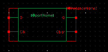
Rising Edge Triggered D-FF Symbol
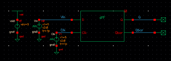
Rising Edge Triggered D-FF Simulation
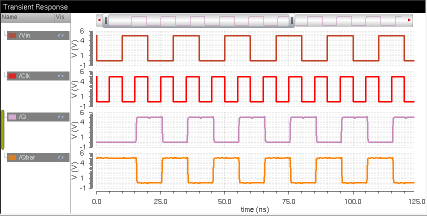
Notice that "Q" only "latches" onto the input "Vin" when the clock is at the rising edge. This is the expected behavior of this component.
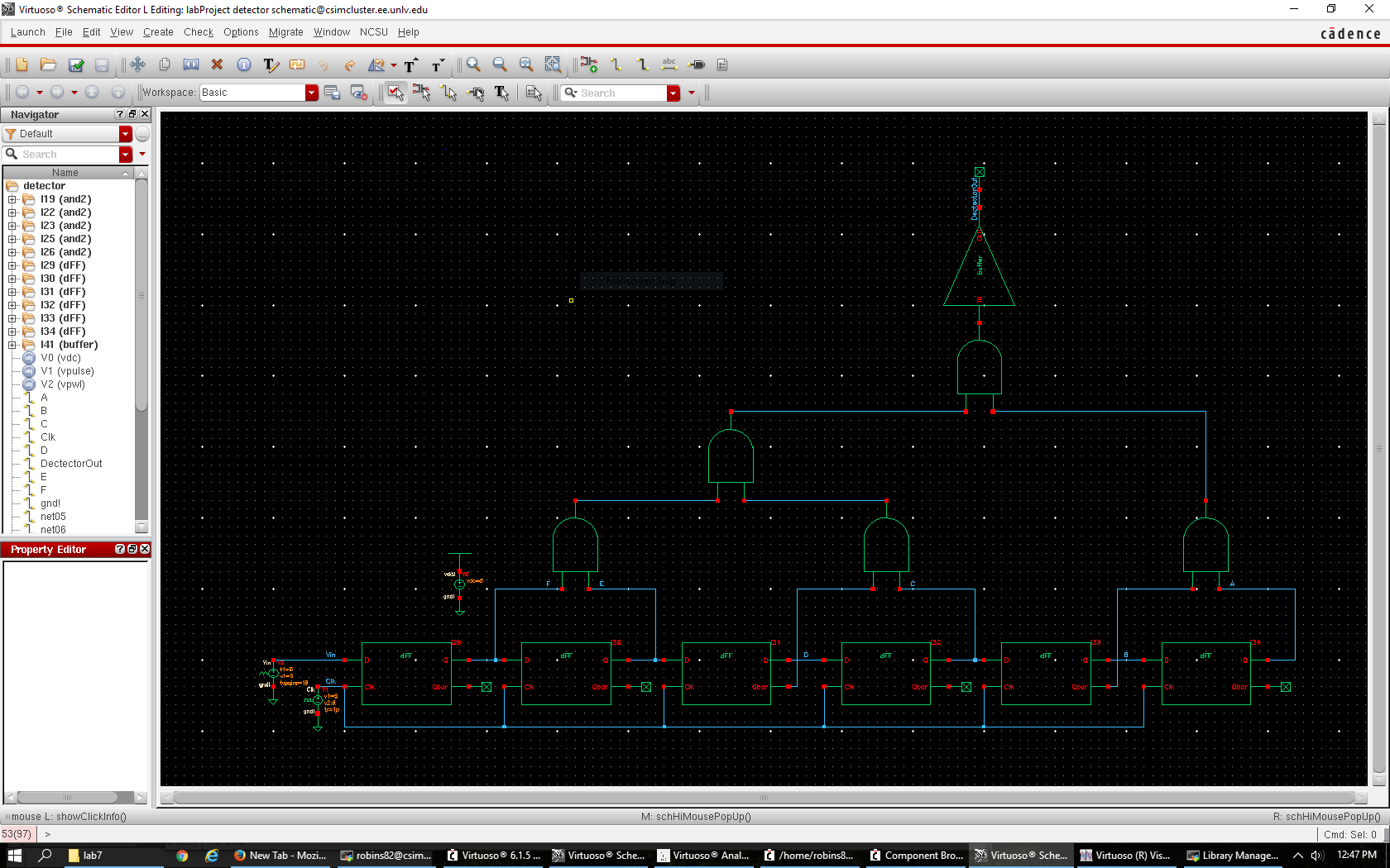
Detector Simulation
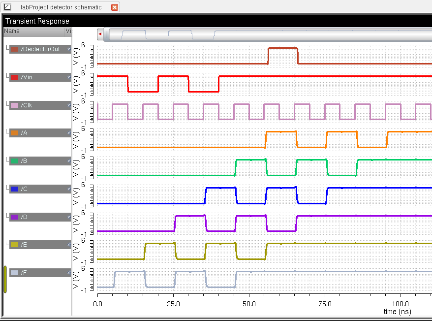
Notice that DectectorOut is only HIGH when the output from the shift register is A . B' . C . D' . E . F (1 0 1 0 1 1 ).
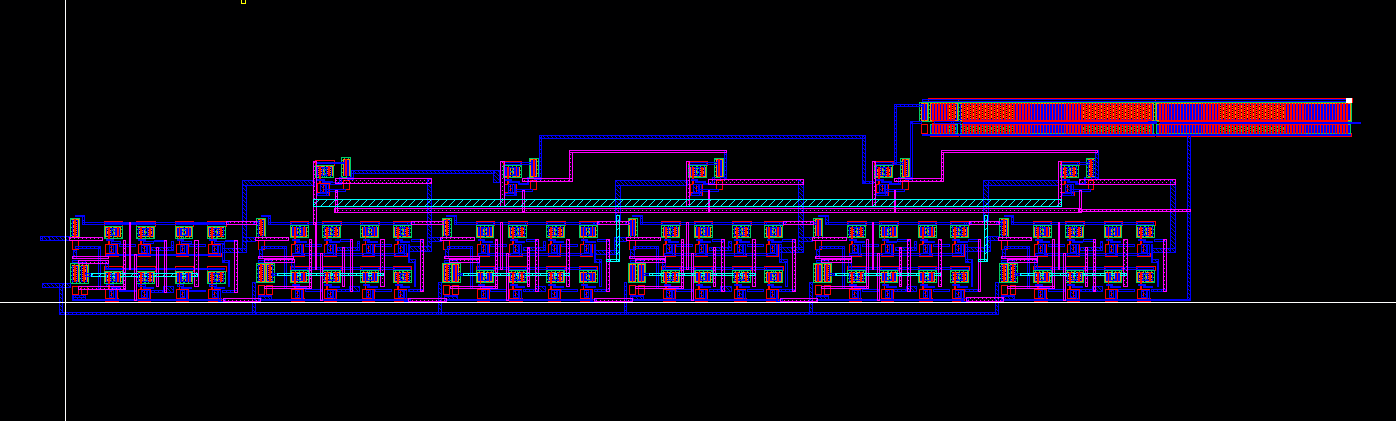
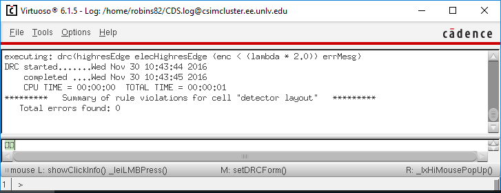
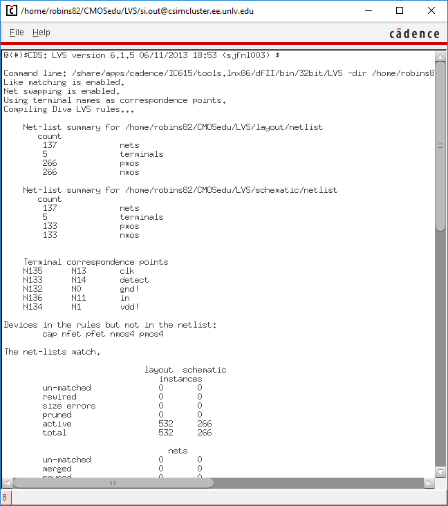
LAYOUTS
Detector:
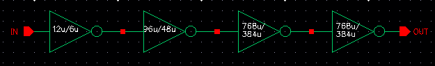
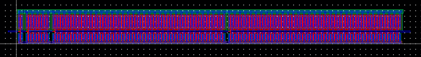
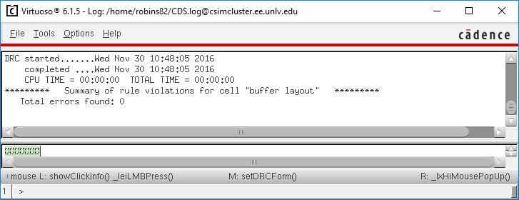
Buffer:
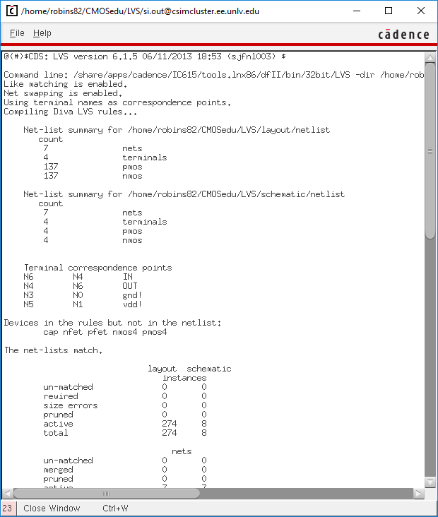
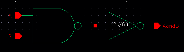
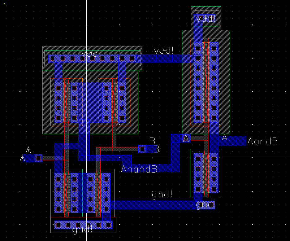
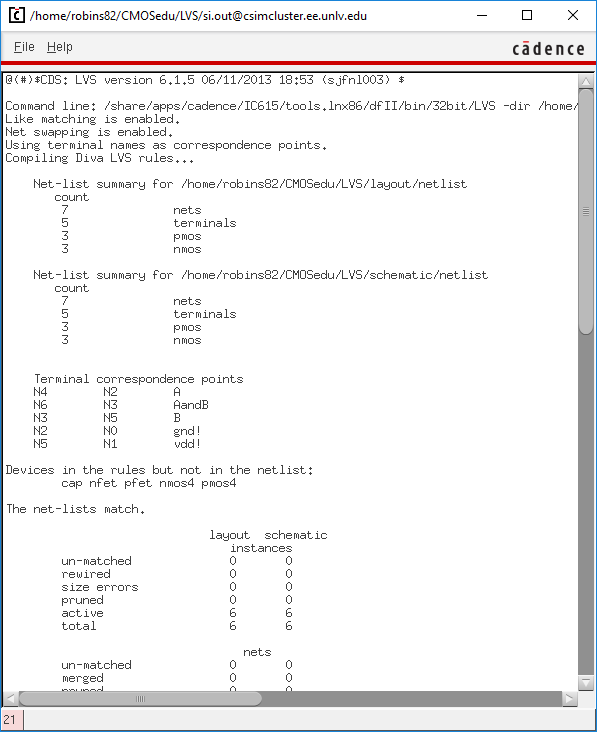
And2:

dff:
Project files located HERE
Return to EE 421L Labs