Lab 7 - ECE 421L
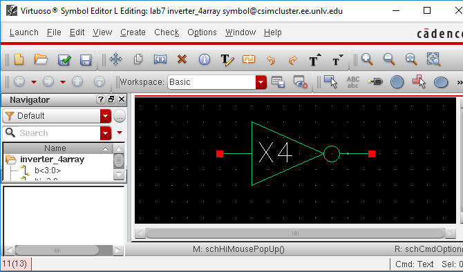
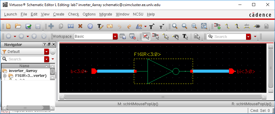
X4 buffer
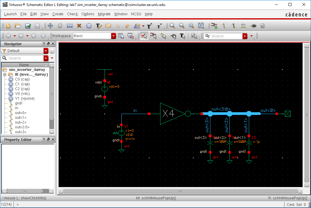
As the load capacitance increases, the delay for the inverter gets larger as seen above.
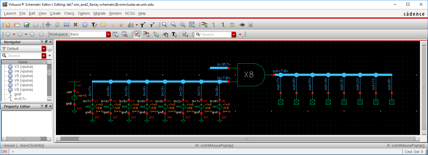
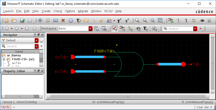
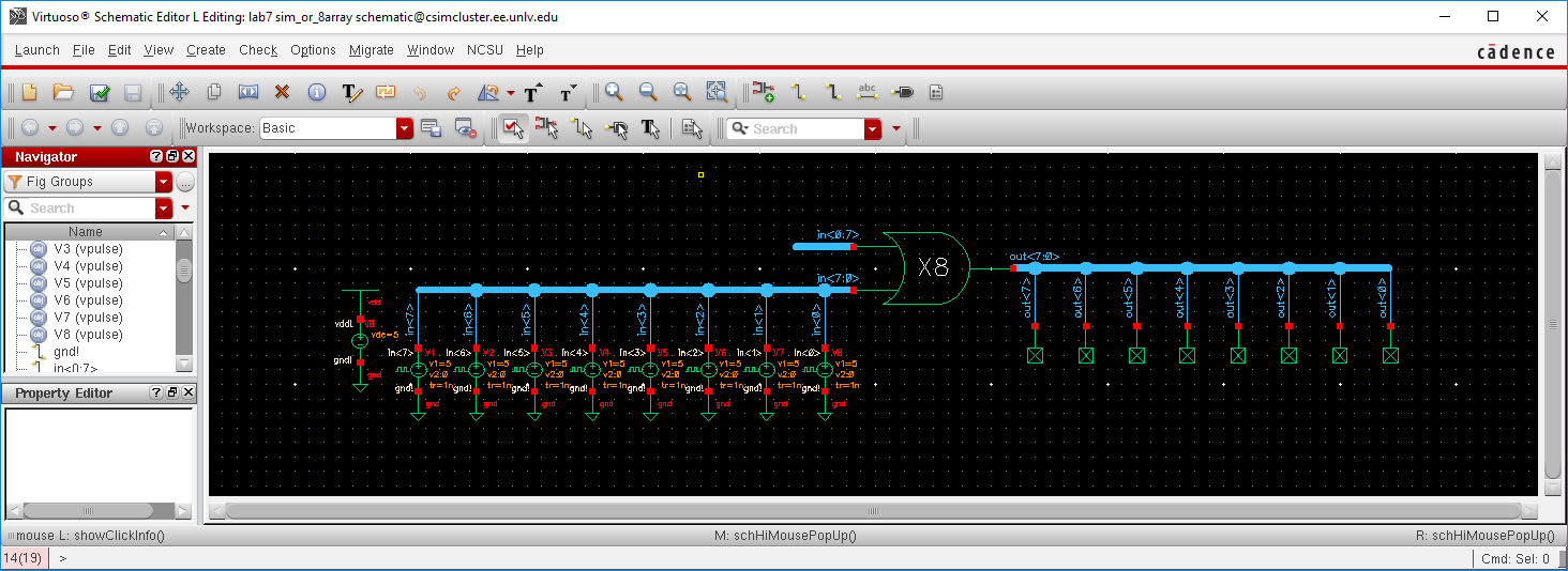
Create schematics and symbols for an 8-bit input/output array of: NAND, NOR, AND, inverter, and OR gates.
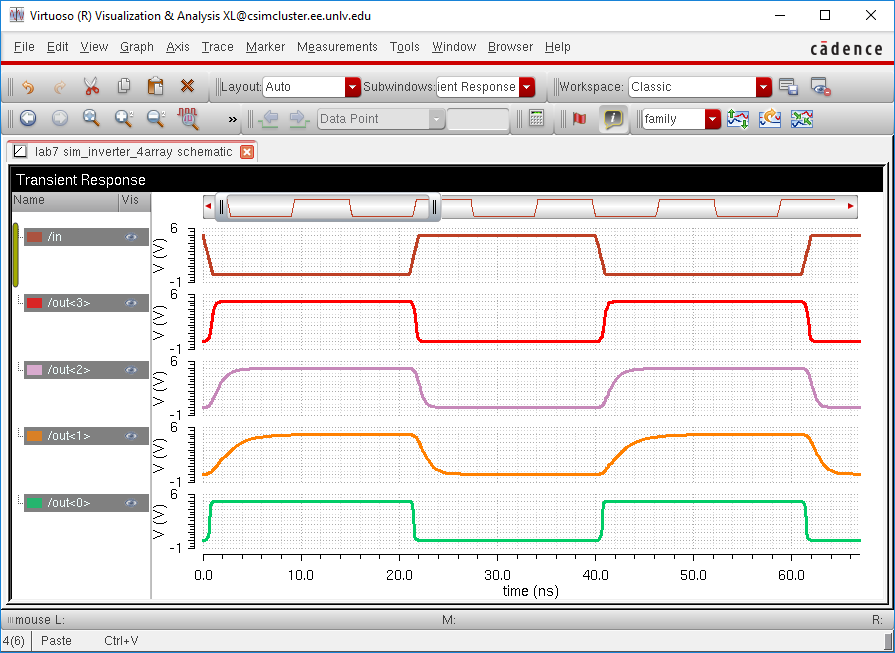
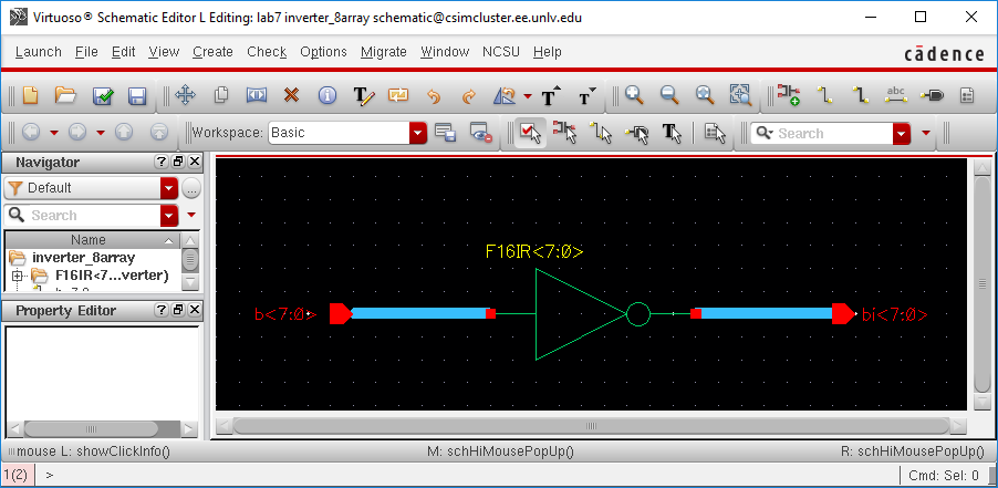
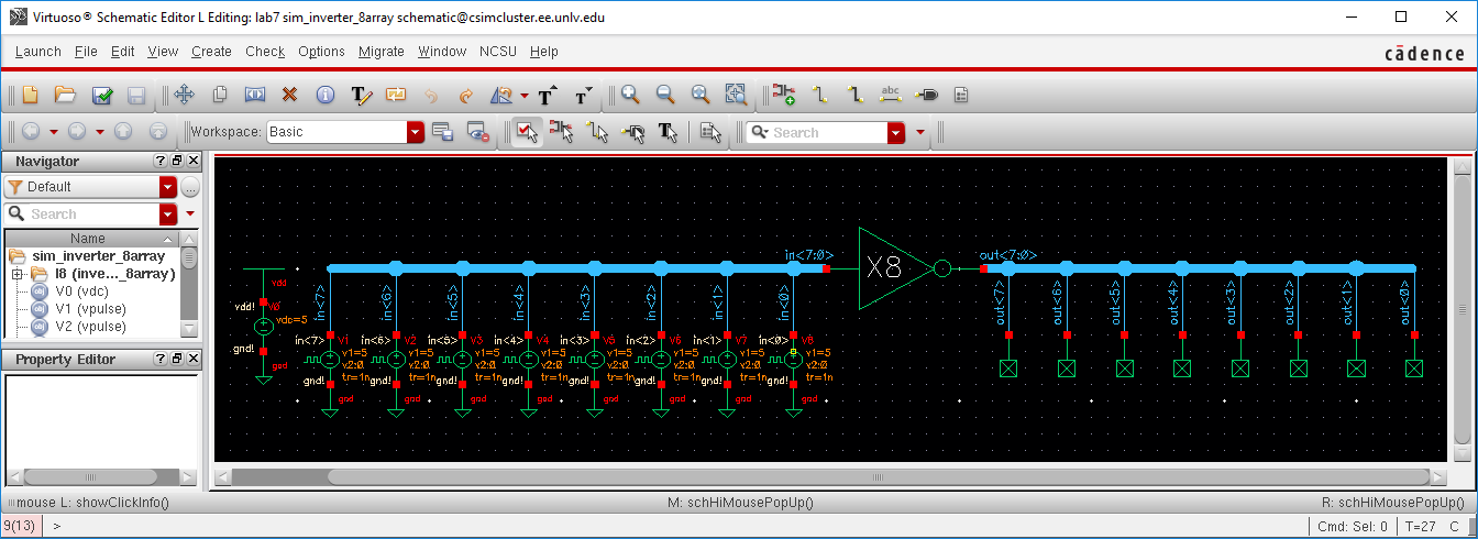
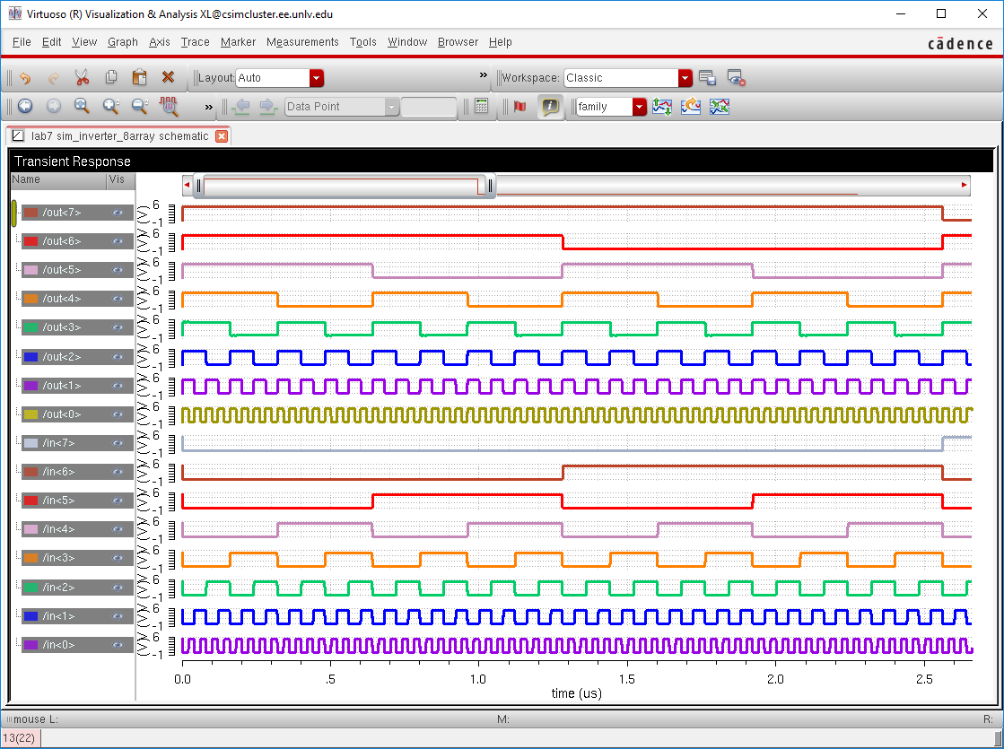
X8 inverter
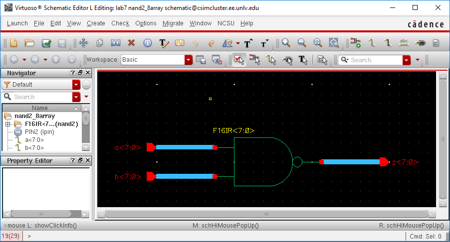
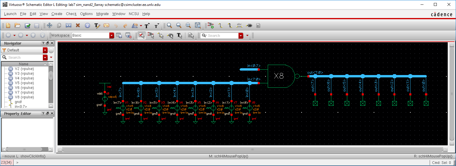
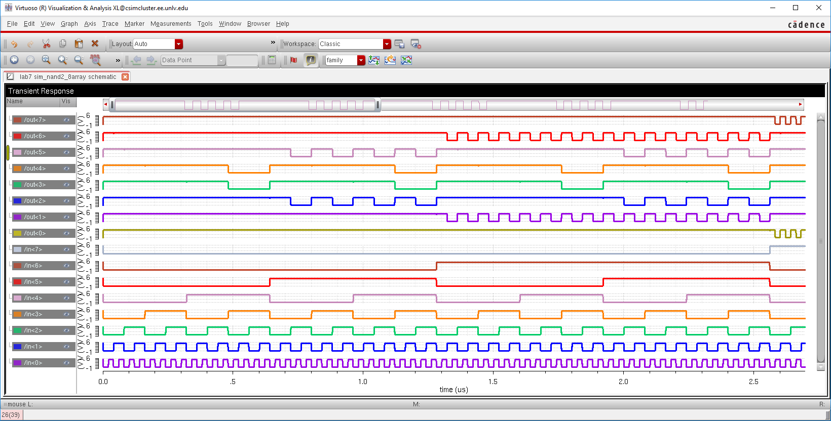
X8 NAND
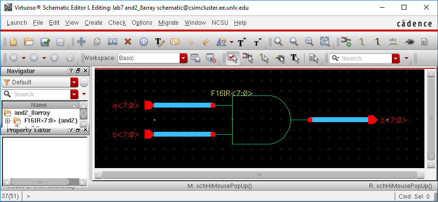
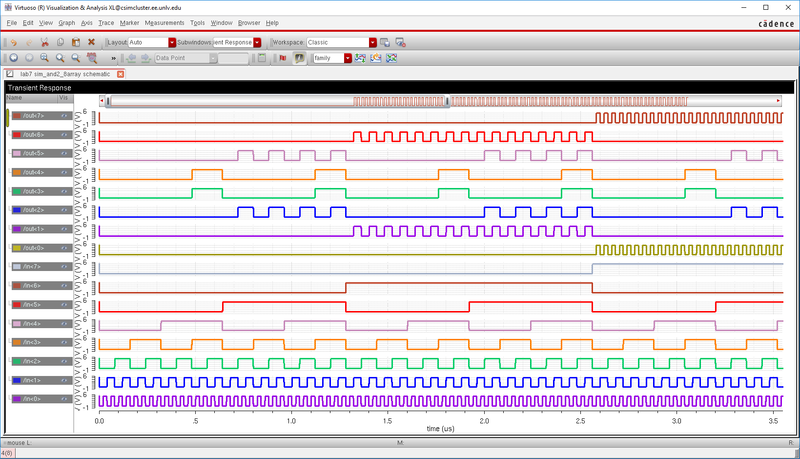
X8 AND
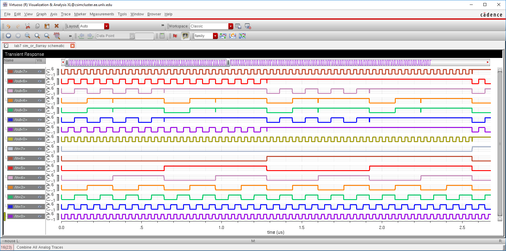
X8 OR
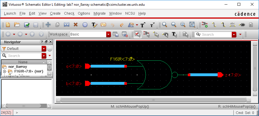
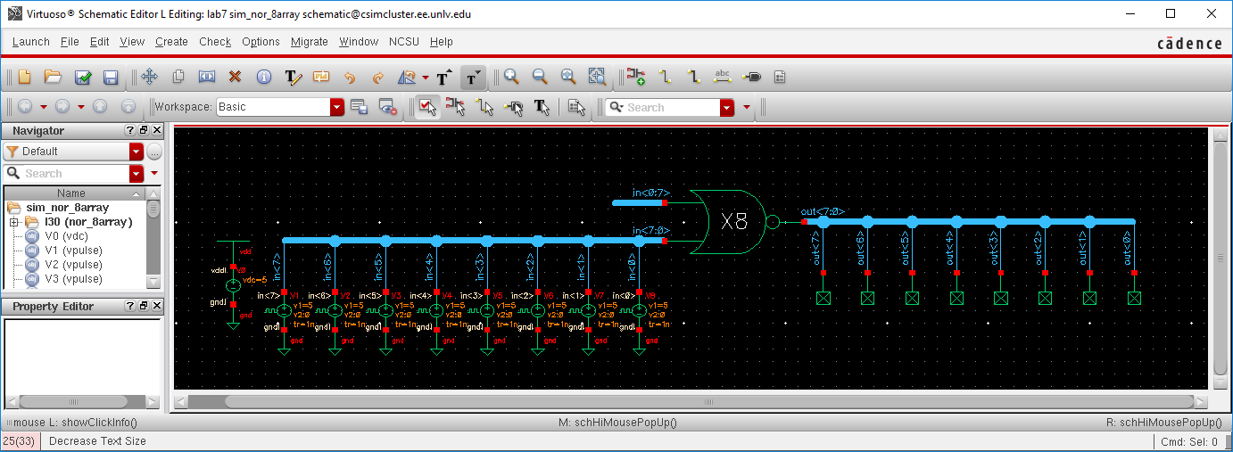
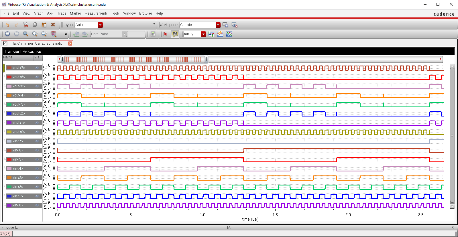
X8 NOR
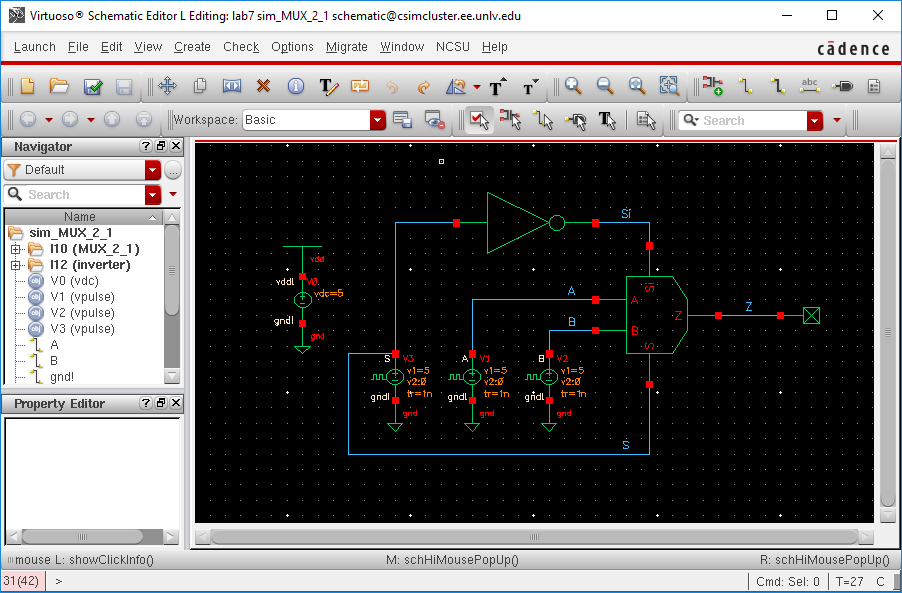
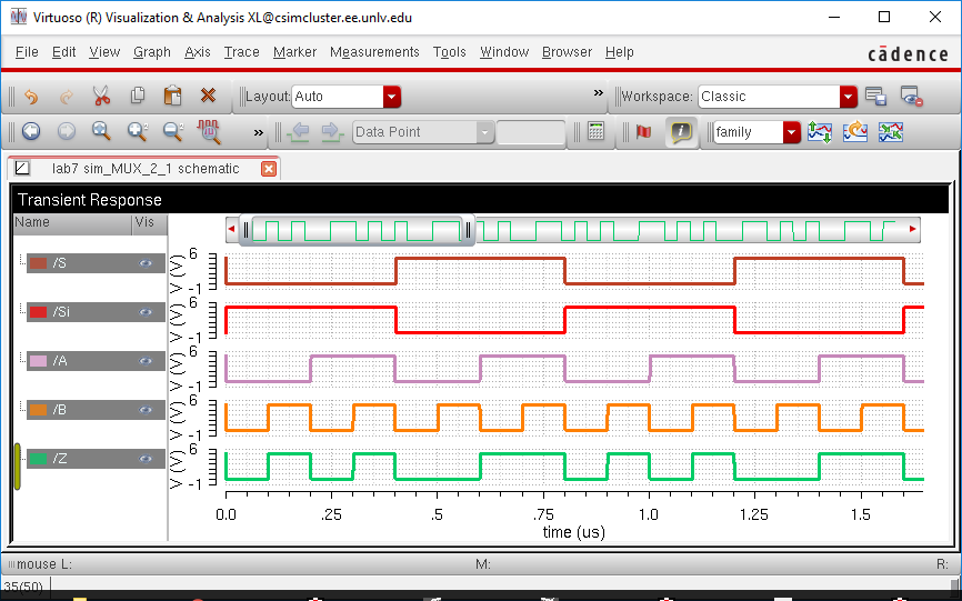
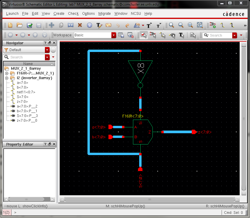
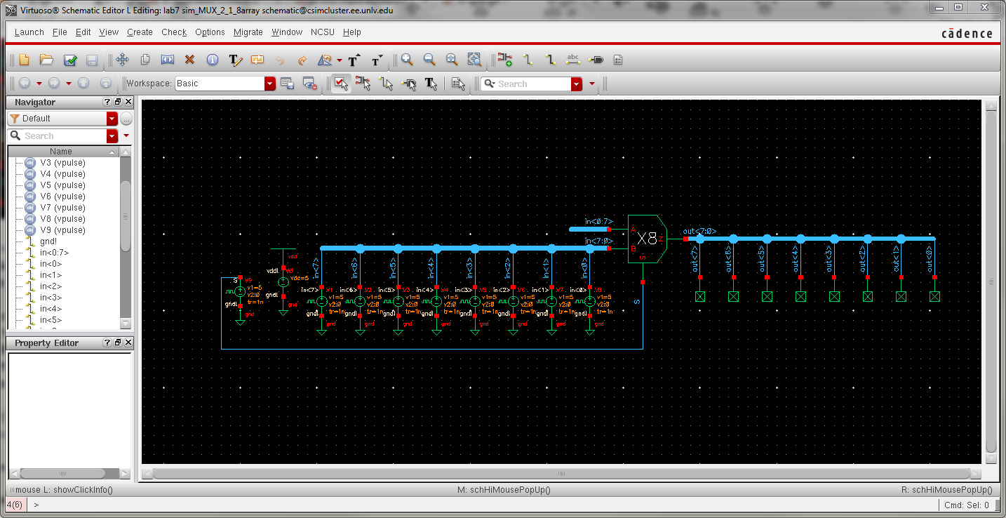
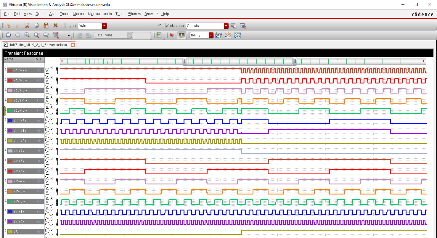
MUX
DEMUX
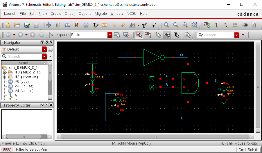
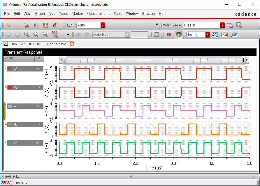
Create an 8-bit wide word 2-to-1 DEMUX/MUX schematic and symbol.
Include an inverter in your design so the cell only needs one select
input, S
(the complement, Si, is generated using an inverter).
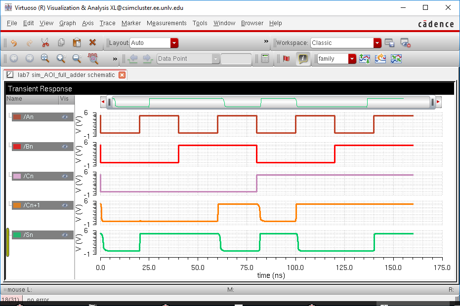
Use simulations to verify the operation of
your
design.
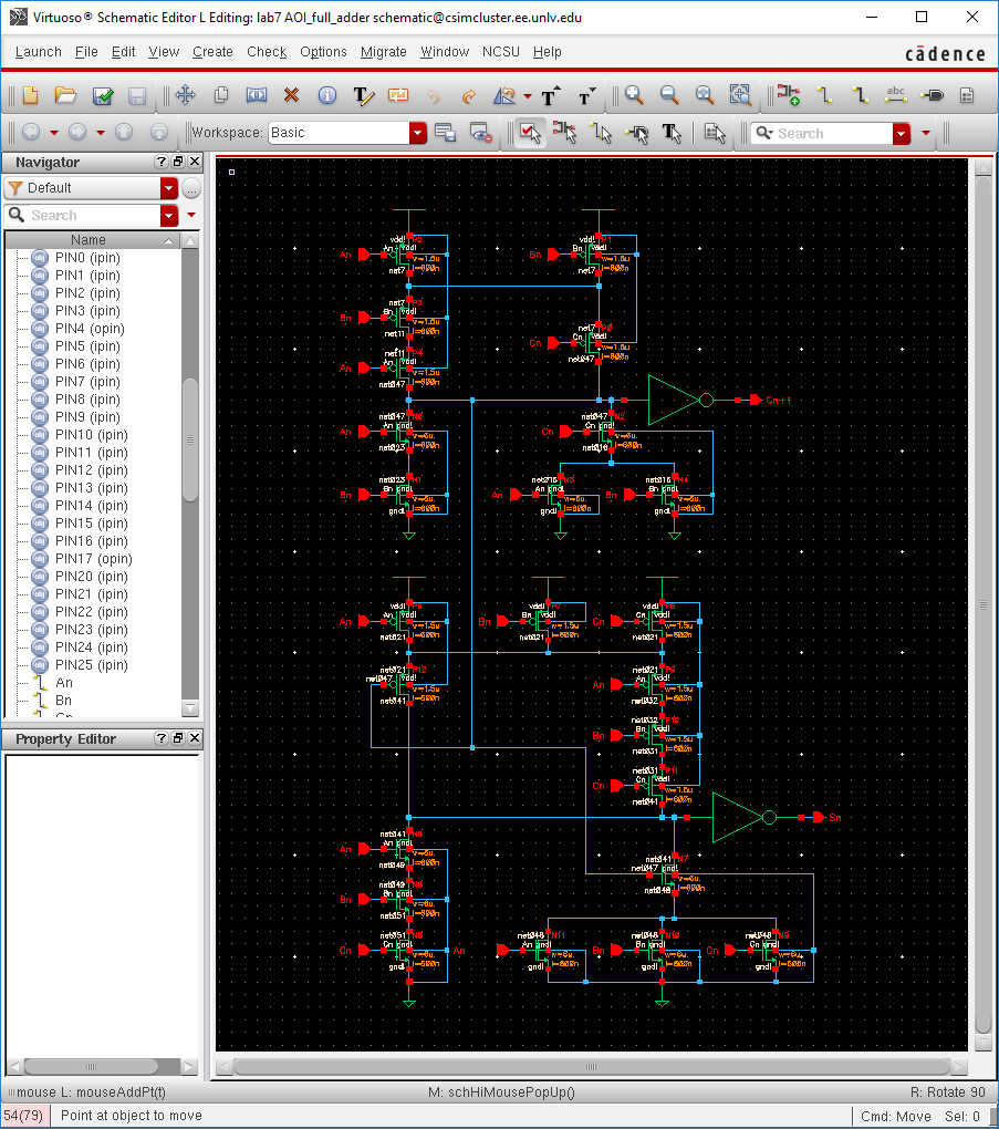
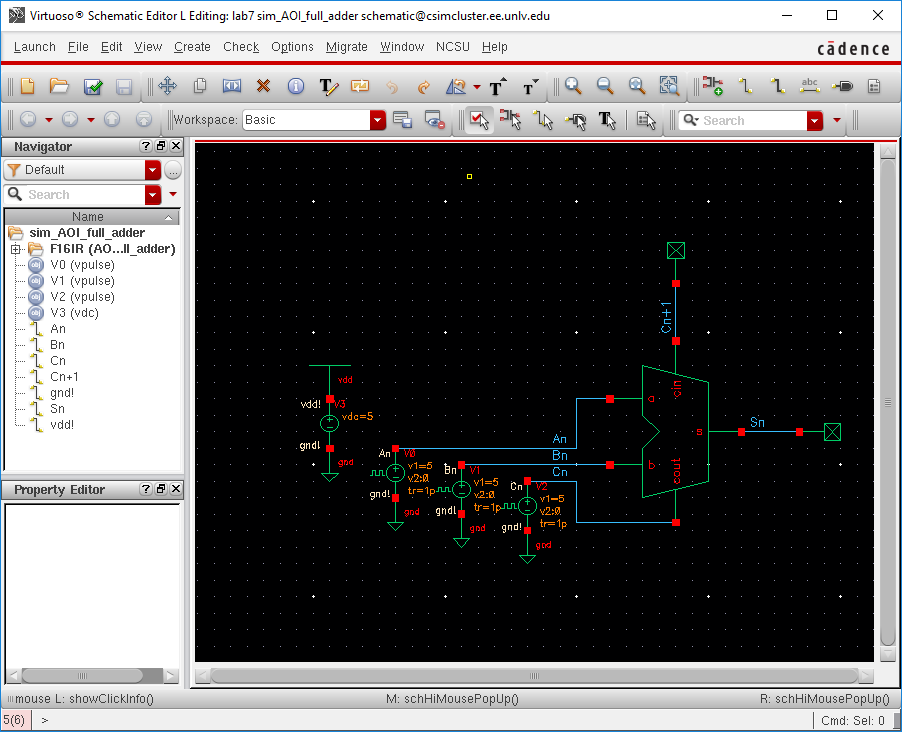
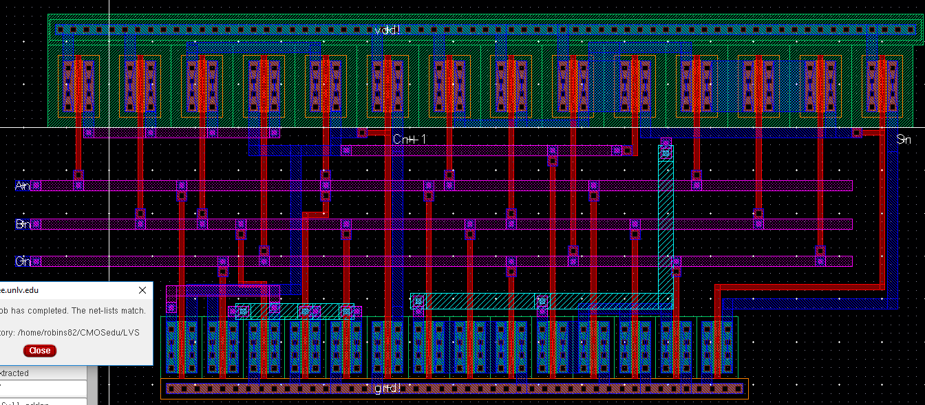
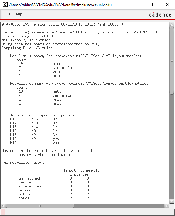
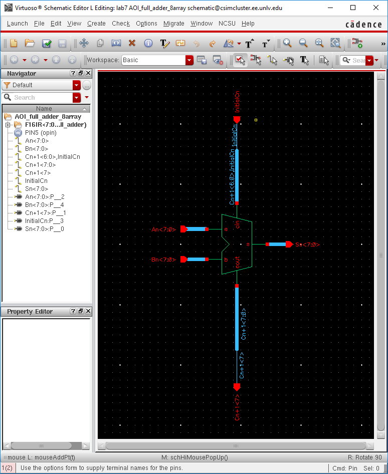
Finally, draft the schematic of the full-adder seen in Fig. 12.20 using
6u/0.6u
devices (both PMOS and NMOS).
Create an adder symbol for this circuit (see the symbol used in lab6).
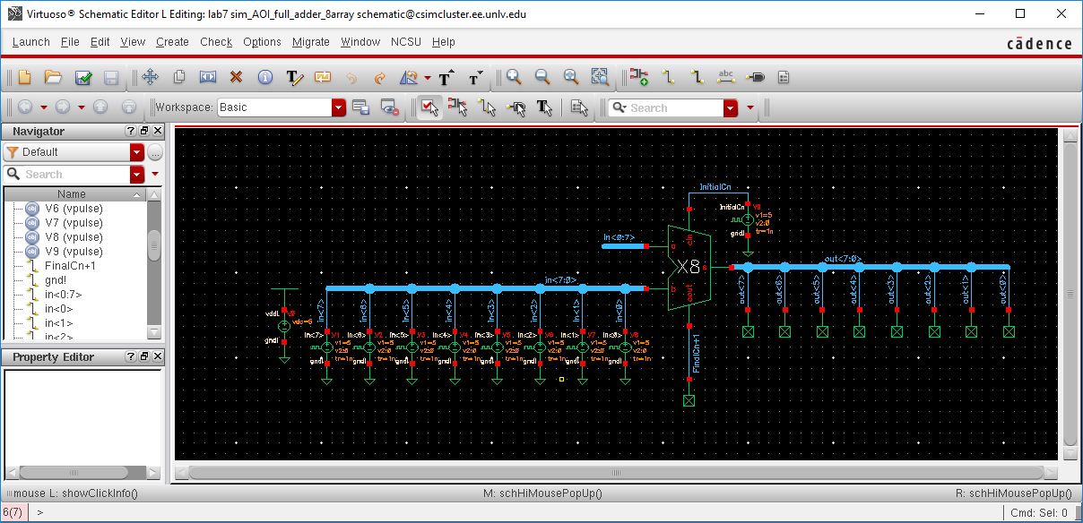
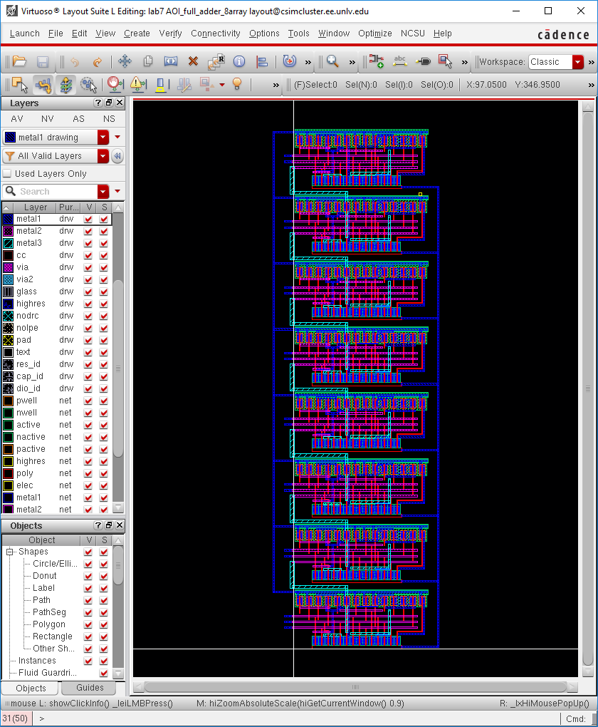
Use this symbol to draft an 8-bit adder schematic and symbol.
For how to label the bus so the carry out of one full-adder goes to the
carry
in of another full-adder review the ring oscillator schematic discussed
in Cadence
Tutorial 5.
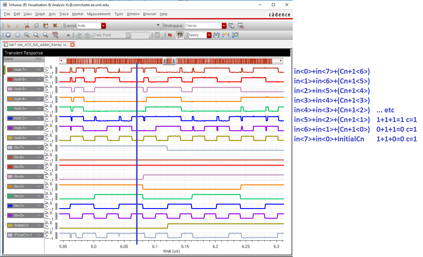
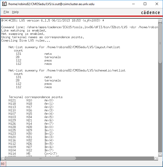
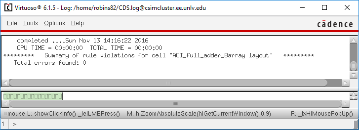
Simulate the operation of your 8-bit adder.
Backup of work