Lab 6 - ECE 421L
Authored
by Isaac Robinson,
robins82@unlv.nevada.edu
October 26th, 2016
This lab focuses on the design, layout, and simulation of a CMOS NAND gate, XOR gate, and Full-Adder
- Draft
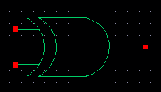
the schematics of a 2-input NAND gate (Fig. 12.1), and a 2-input XOR
gate (Fig. 12.18) using 6u/0.6u MOSFETs (both NMOS and PMOS)
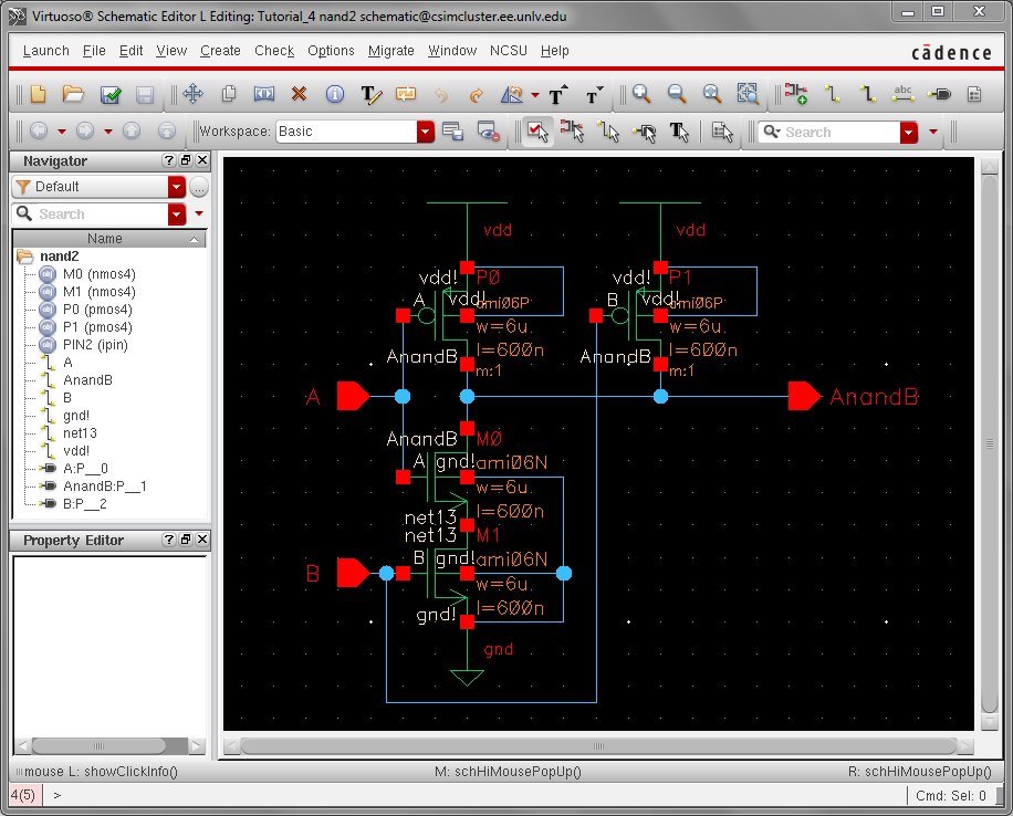
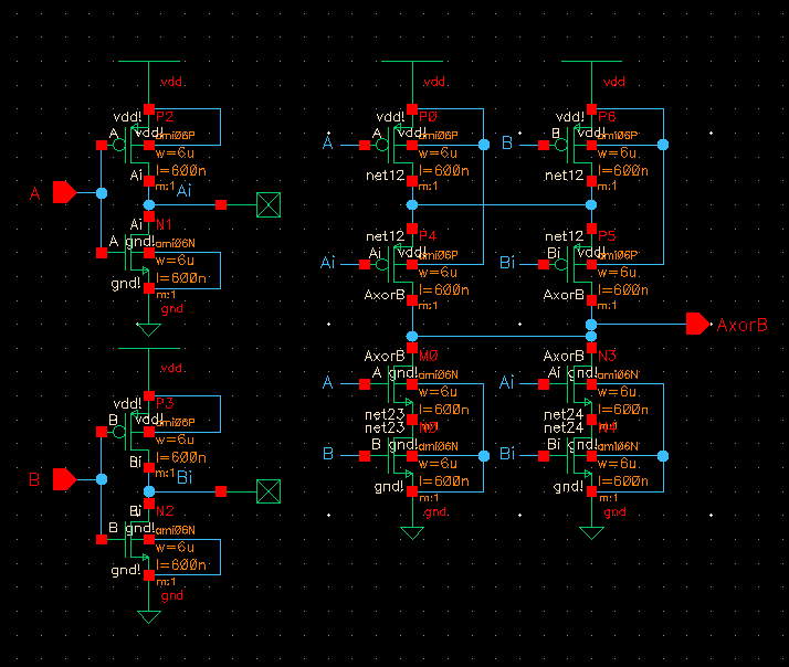
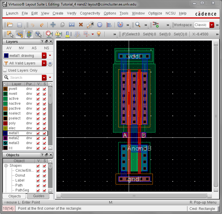
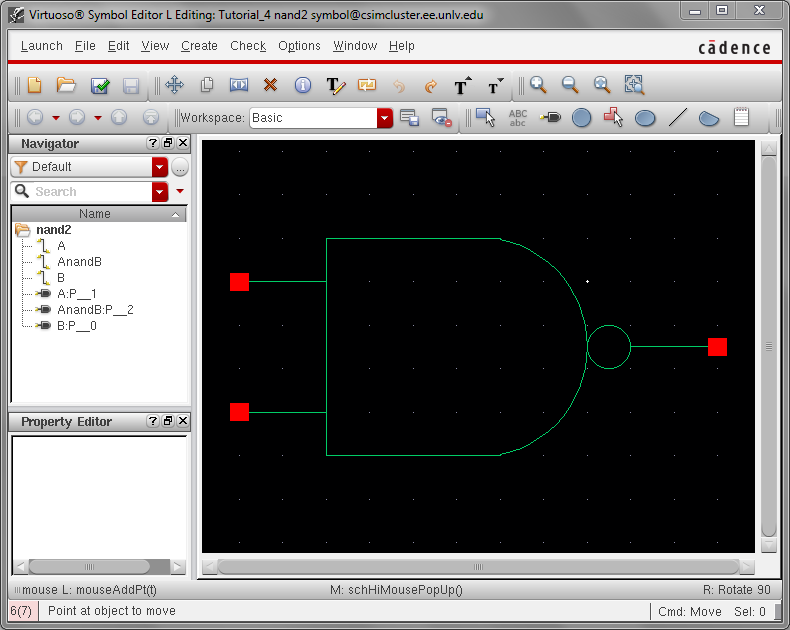
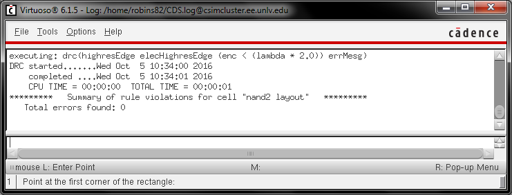
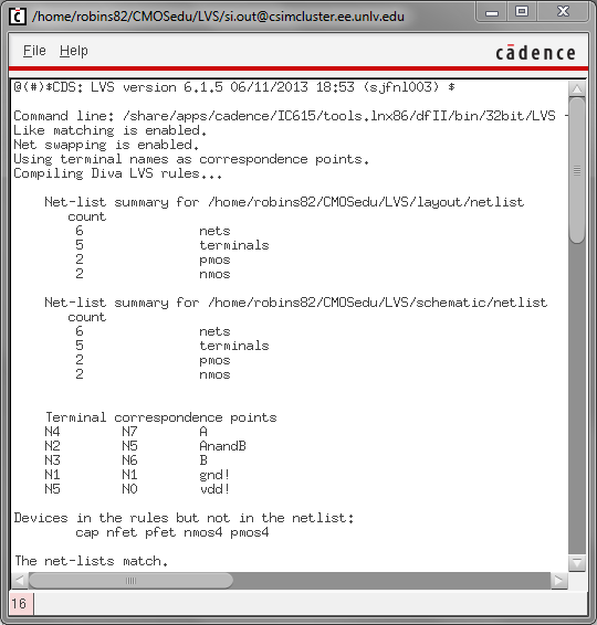
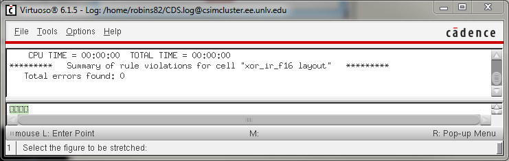
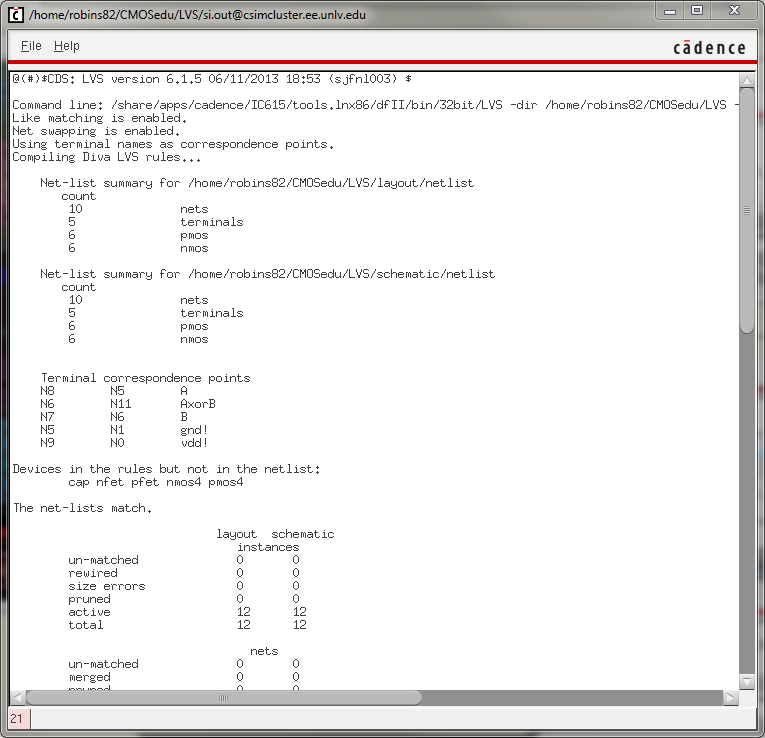
- Create layout and symbol
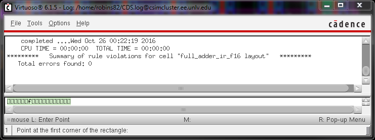
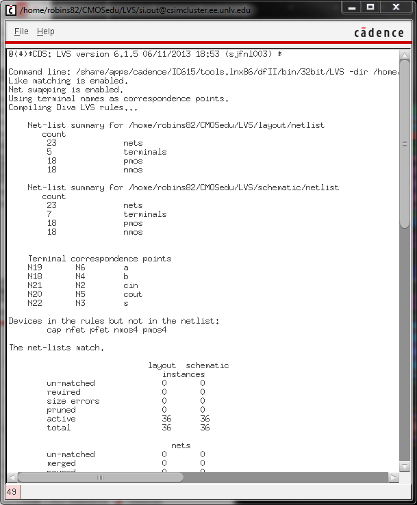
views for these gates showing that the cells DRC and LVS
without errors
- ensure that your symbol
views are the commonly used symbols (not boxes!) for these gates with your initials in the middle of the symbol
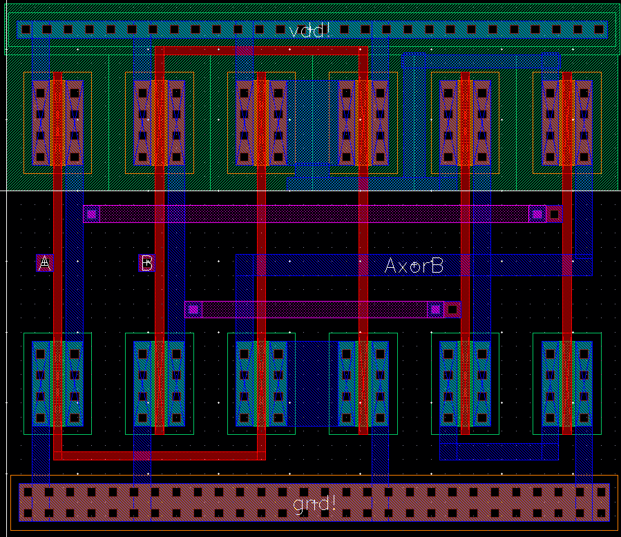
- ensure all layouts in
this lab use standard cell frames
that snap together end-to-end for routing vdd!
and gnd!
- use a standard cell height taller than you
need for these gates so that it
can be used for more complicated layouts in the future
- ensure gate inputs,
outputs, vdd!, and gnd! are all routed on metal1
NAND ---------
XOR ---------
- Use cell names that
include your initials and the current year/semester, e.g. NAND_jb_f19
(if it were fall 2019)
- Using Spectre simulate the logical operation of the gates for all 4 possible
inputs (00, 01, 10, and 11)
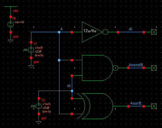
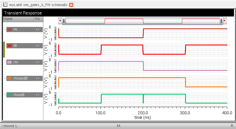
- comment on how timing of the input pulses can cause glitches in the output of a gate
- Your html lab report
should detail each of these efforts
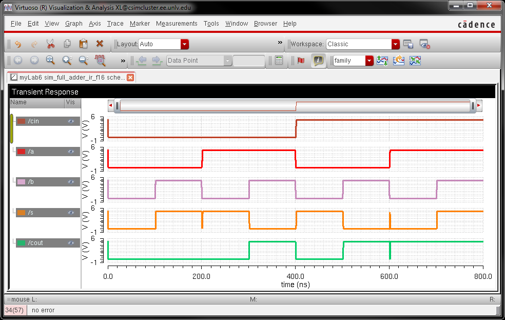
As
we can see from the simulation of the gates, when both inputs are
opposite values and get inverted on the same clock edge the output of
the XOR gate drops during this period. This is because the
rising/falling edge of the clock happen during a period of t. Ideally,
if t <- 0 then we would not see this behavior coming from the MOSFET
based XOR gate.
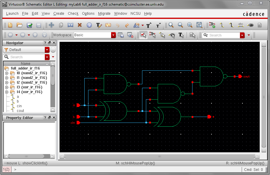
- Using these gates, draft the schematic of the full adder
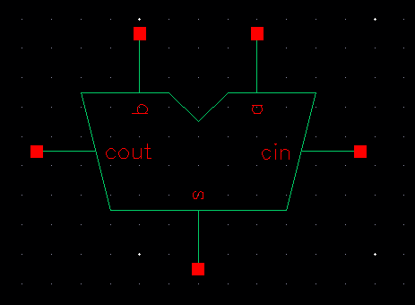
- Create a symbol for
this full-adder (example)
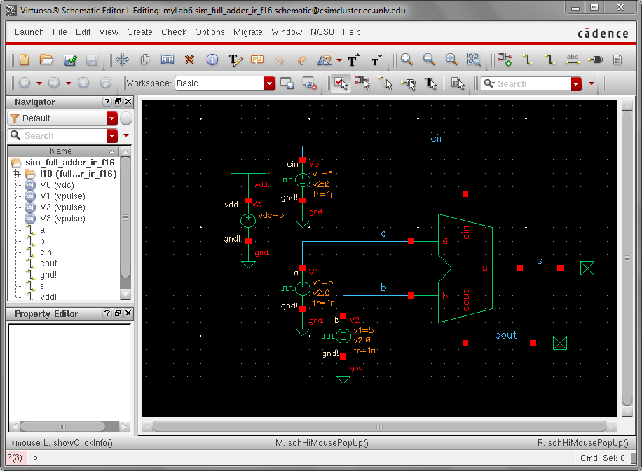
- Simulate,
using Spectre, the operation of the
full-adder using this symbol
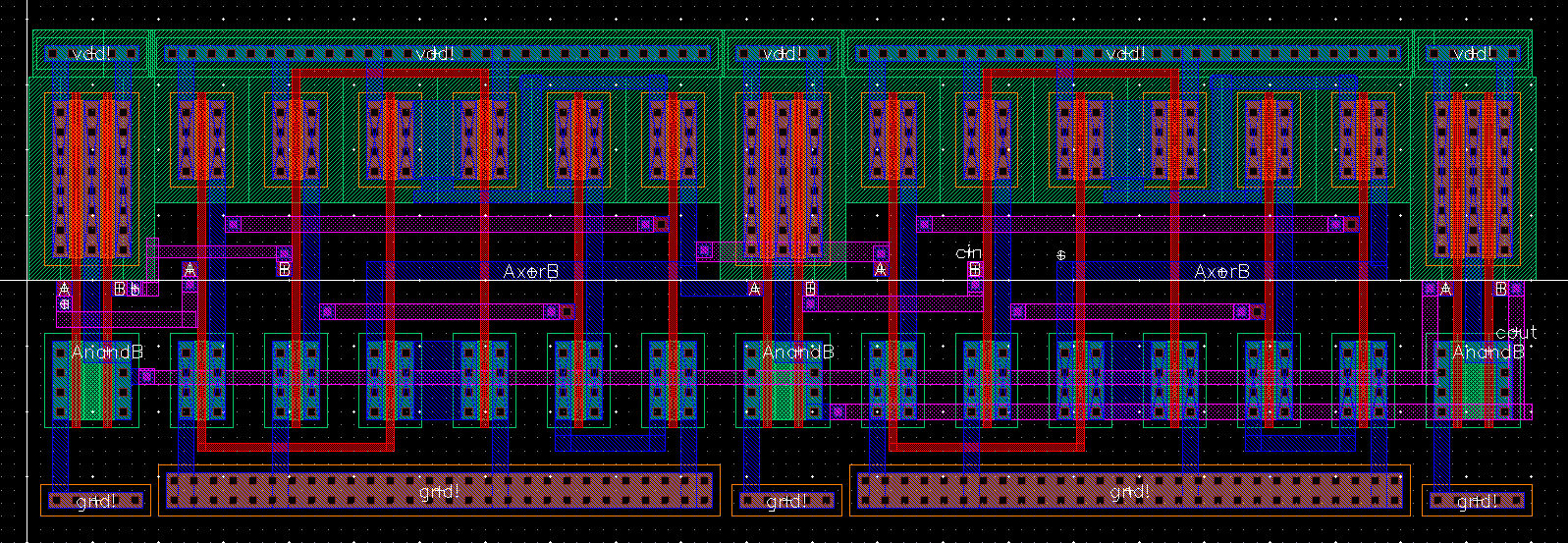
- Layout the full-adder
by placing the 5 gates end-to-end so that vdd! and gnd! are routed
- full-adder inputs and
outputs can be on metal2 but not metal3
- DRC and LVS your full adder design
BACKUP:
My lab6 files are located HERE for review.Return to Isaac's Labs
Return to EE 421L Labs