Lab 5 - ECE 421L
Authored
by Isaac Robinson,
robins82@unlv.nevada.edu
October 5th, 2016
This lab focuses on the design, layout, and simulation of a CMOS inverter.
- Draft schematics,
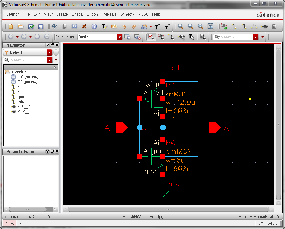
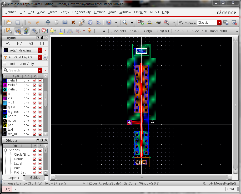
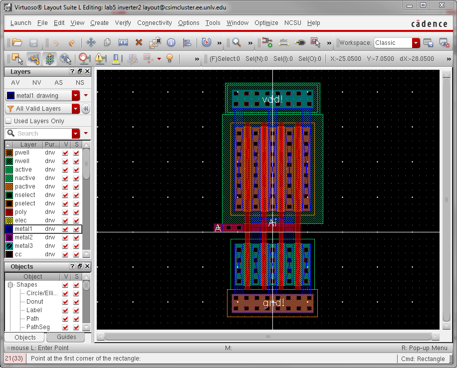
layouts, and symbols for two inverters having sizes of:
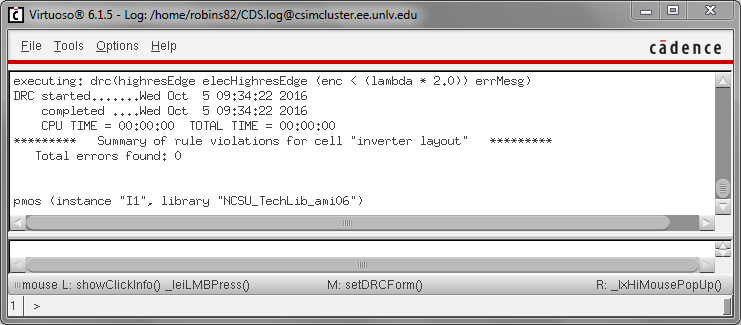
- 12u/6u (= width of the
PMOS / width of the NMOS with both devices having minimum lengths of 0.6u
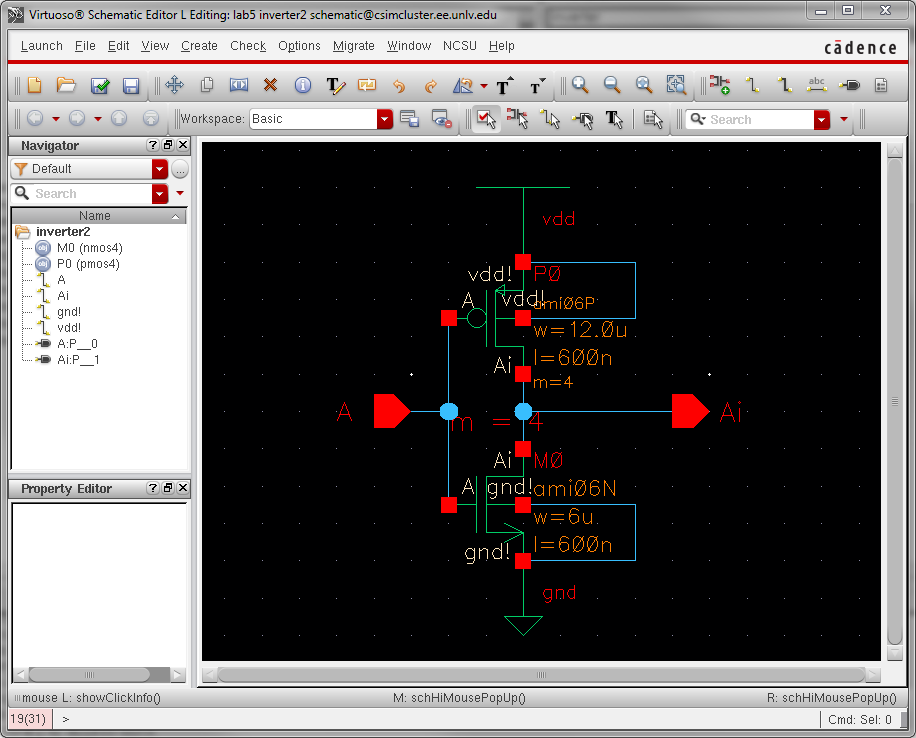
- 48u/24u where the devices use a multiplier, M = 4
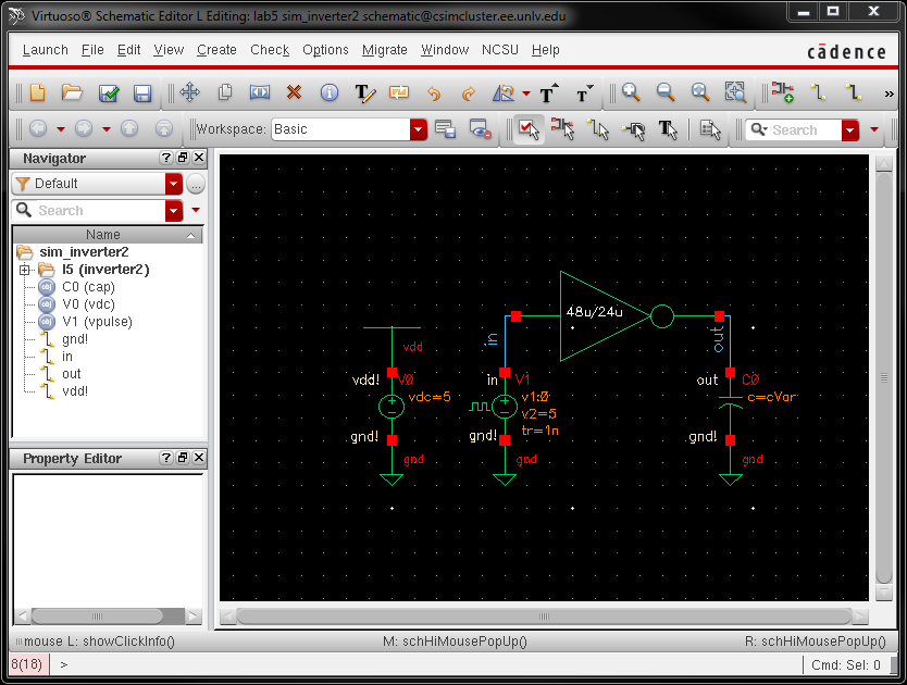
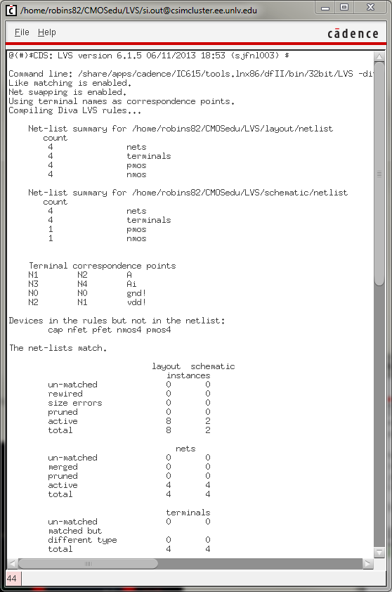
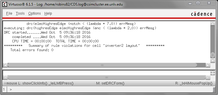
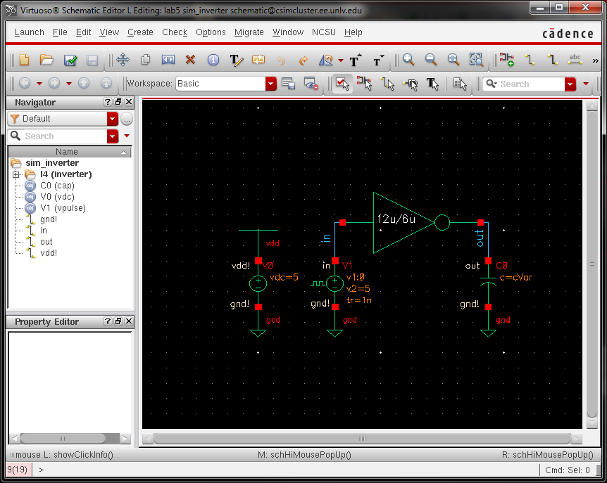
- Using SPICE simulate
the operation of both of your inverters showing each driving a 100 fF, 1 pF, 10 pF, and 100 pF capacitive load
- 12u/6u ===============================================
- What
can be observed in the following image is the impact of a capactior on
the 12u/6u inverter circuit. At 100fF the inverter functions as
desired, but as this capitance increases, the reaction time for the
output decreases. At above 1pF the inverter is not even given enough
time to reach the ideal max output voltage.
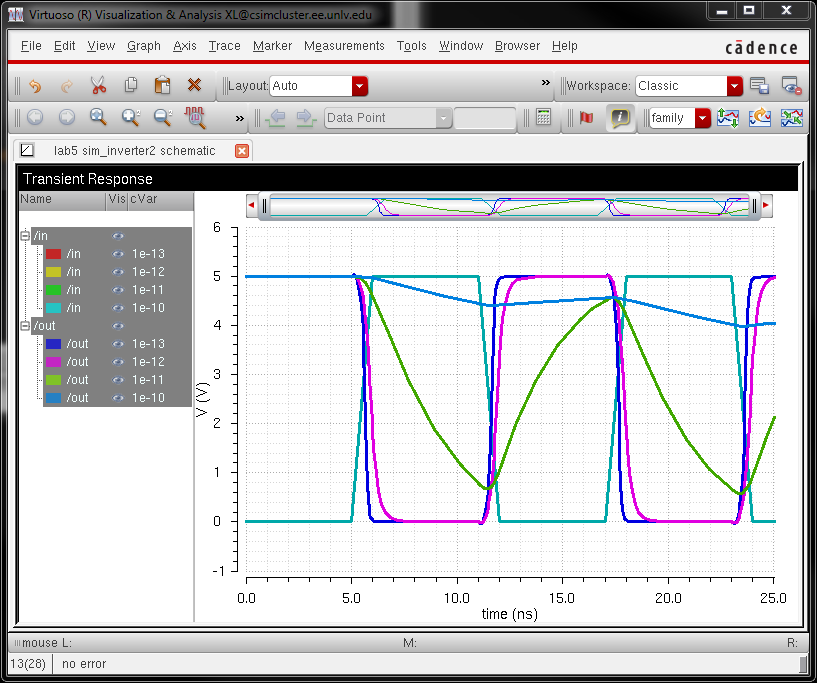
- 48u/24u
- The
same observations are made for the following image. But in this case
the voltages seem to get a little closer to ideal voltage for the
inverter.
- Comment, in your
report, on the results
- Use UltraSim (Cadence's fast SPICE simulator for larger circuits at the cost of accuracy) and repeat the above simulations
- Use Setup -> Simulator/Directory/Host and select UltraSim as seen below
- You'll also have to point to the MOSFET models again as seen below
- Note that UltraSim only performs transient simulations (not AC, Noise, DC, operating point, etc.)
- Not knowing this last item will lead to wasted time if trying to use UltraSim exclusively for simulations
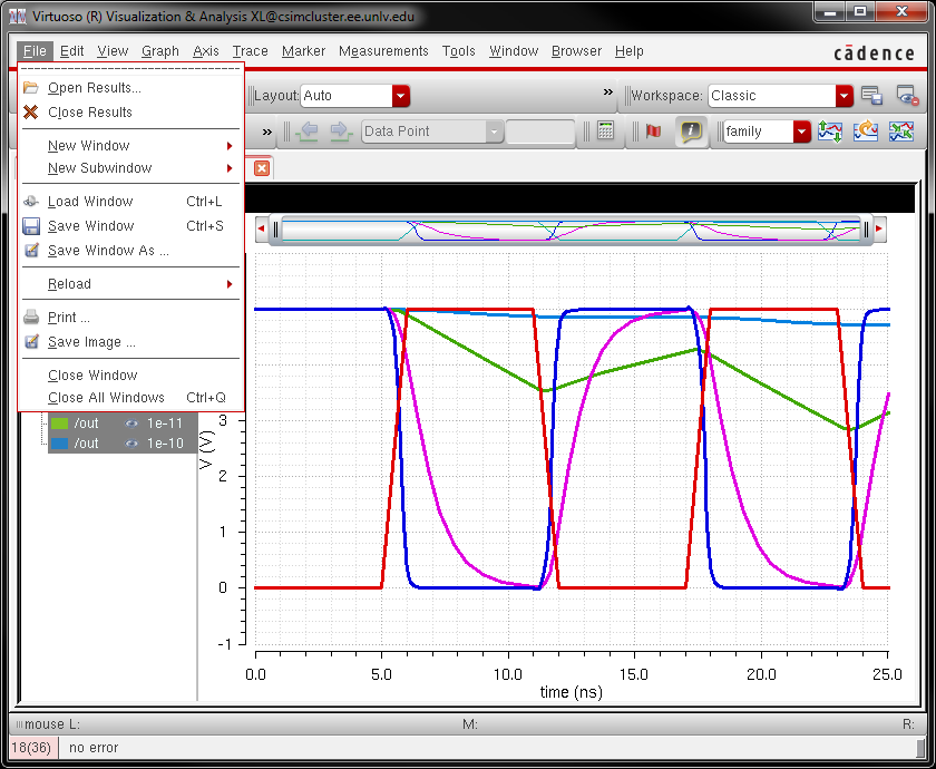
- 12u/6u =======================================================
- The result here is very simular to the one above for 12u/6u
- 48u/24u =======================================================
- Just like the results for 12u/6u, these are very similar to the simulation done in previous section for 48u/24u
 When finished backup your work (webpages
and design
directory).

Return to Isaac's Labs
Return to EE 421L Labs