Lab 4 - ECE 421L
Authored
by Isaac Robinson,
robins82@unlv.nevada.edu
September 28th, 2016
This lab focuses on IV characteristics and layout of NMOS and POMOS devices in ON's C5 process.
- Generate 4
schematics and simulations (see the examples in the Ch6_IC61 library, but note that for the PMOS body should be at vdd! instead of gnd!):
- A
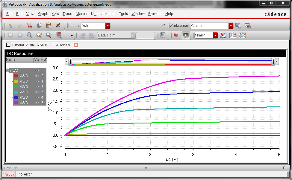
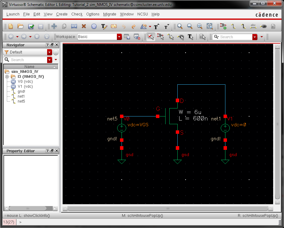
schematic for simulating ID v. VDS of an NMOS device for VGS varying from
0 to 5 V in 1 V steps while VDS varies from 0 to 5 V in 1 mV steps. Use a 6u/600n width-to-length ratio.
- A
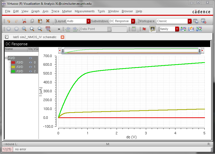
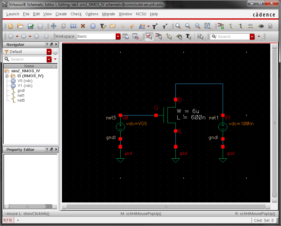
schematic for simulating ID v. VGS of an NMOS device for VDS = 100 mV
where VGS varies from 0 to 2 V in 1 mV steps. Again use a 6u/600n width-to-length ratio.
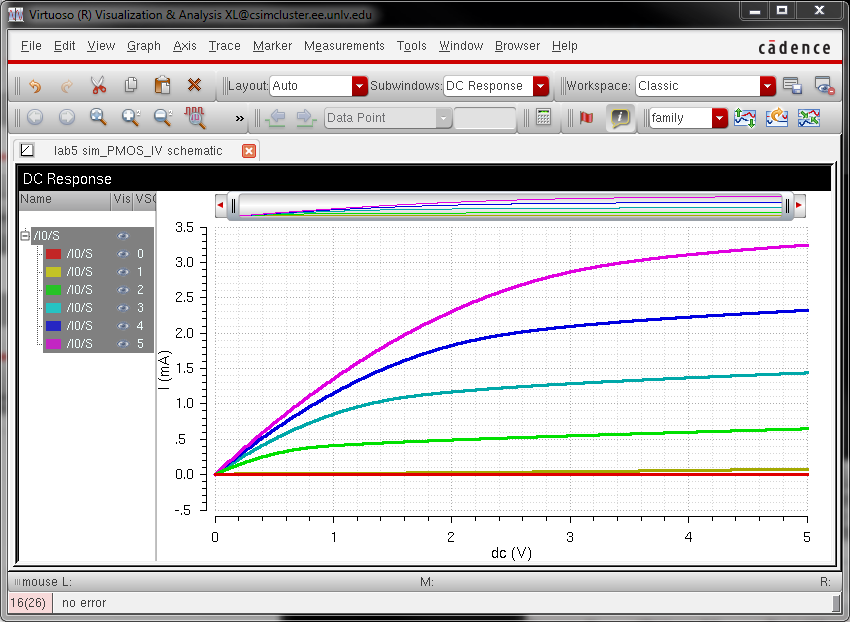
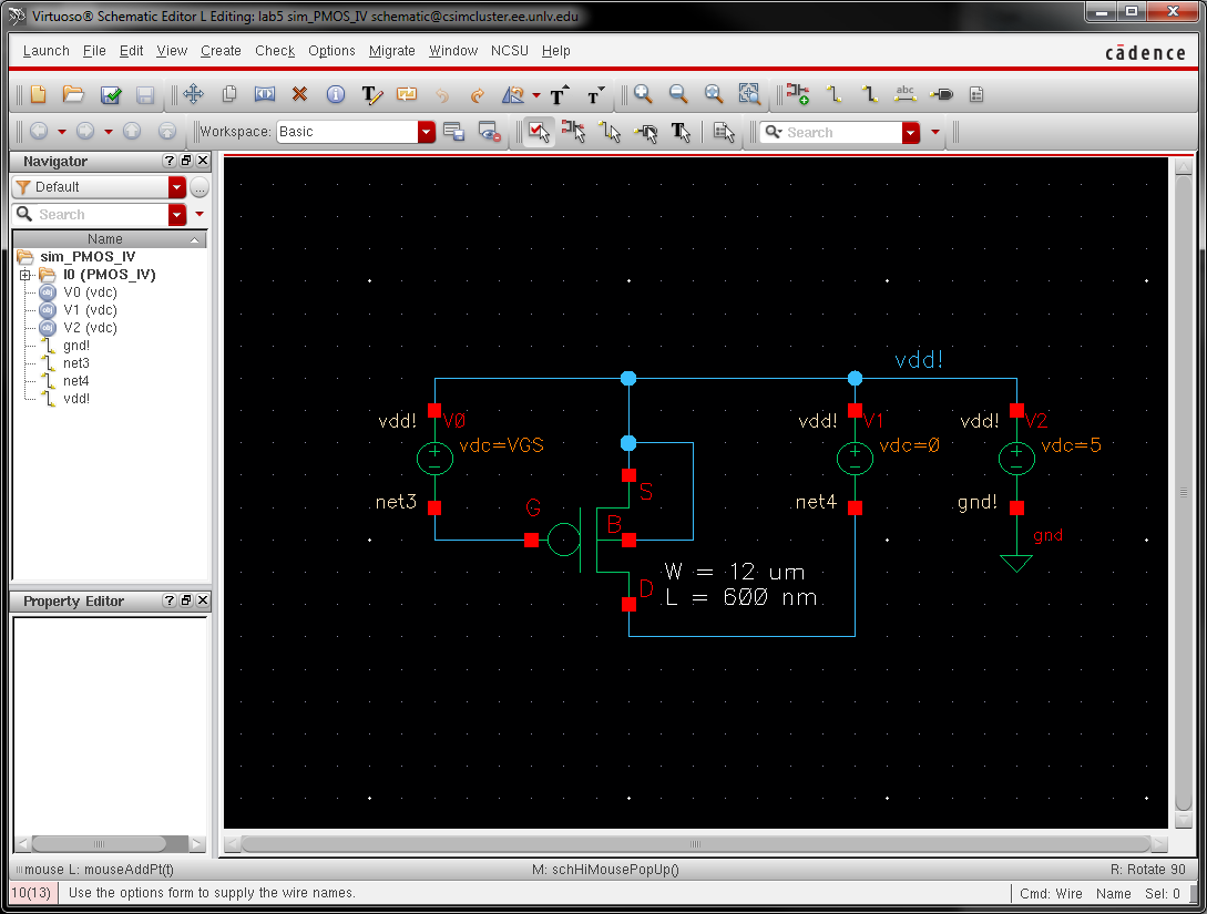
- A
schematic for simulating ID v. VSD (note VSD not VDS) of a PMOS device
for VSG (not VGS) varying from 0 to 5 V in 1 V steps while VSD varies
from 0 to 5 V in 1 mV steps. Use a
12u/600n width-to-length ratio.
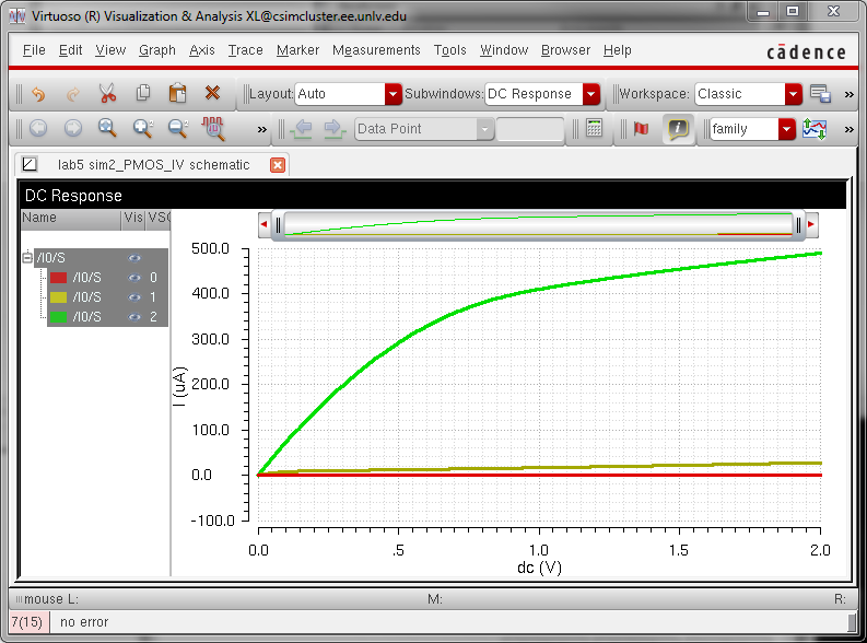
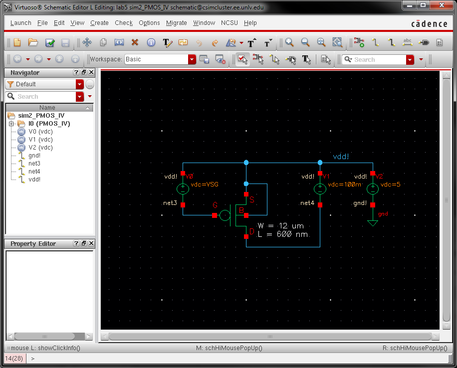
- A
schematic for simulating ID v. VSG of a PMOS device for VSD = 100 mV
where VSG varies from 0 to 2 V in 1 mV steps. Again, use a 12u/600n width-to-length ratio.
` 
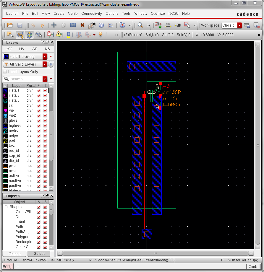
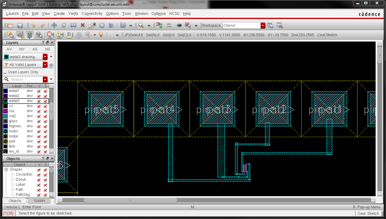
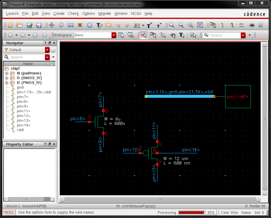
- Lay out a
6u/0.6u NMOS device and connect all 4 MOSFET terminals to probe pads
(which can be considerably smaller than bond pads [see MOSIS design rules]
and directly adjacent to the MOSFET (so the layout is relative small).
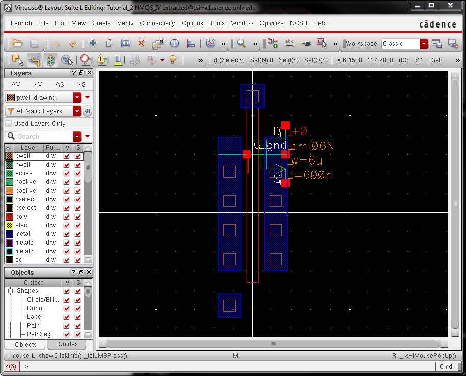
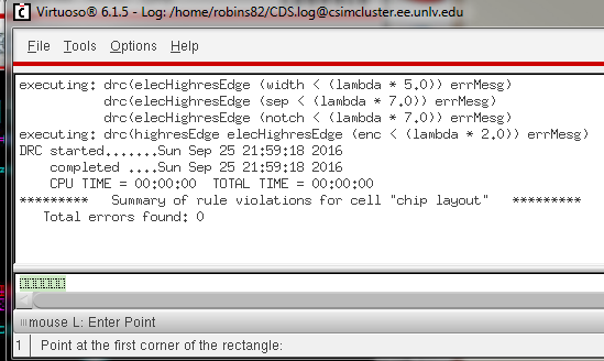
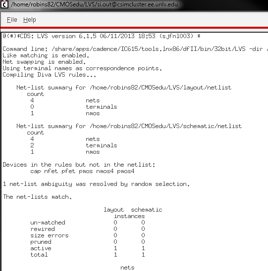
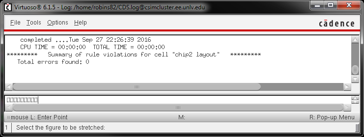
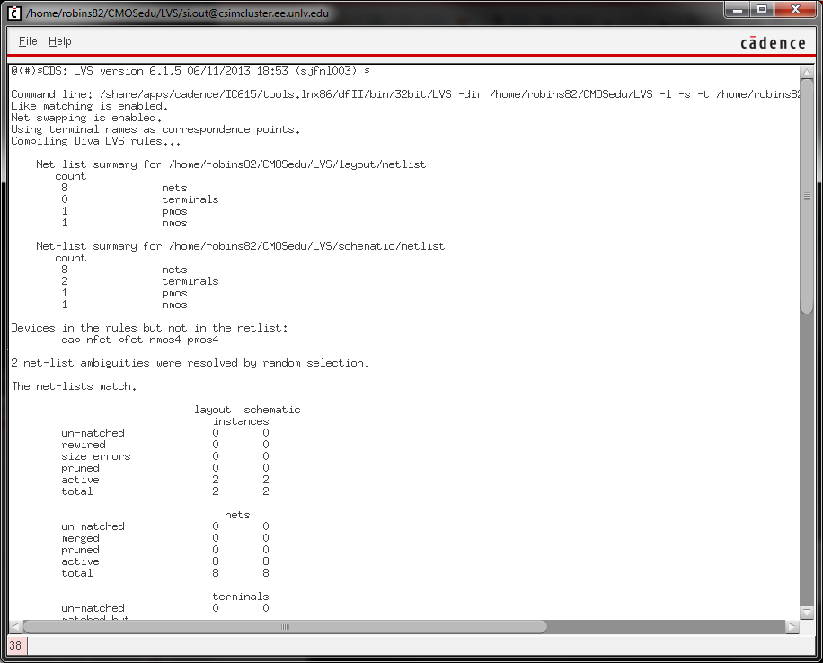
- Show your layout passes DRCs.
- Make a corresponding schematic so you
can LVS your layout.
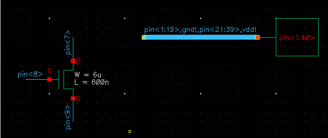
Lay out a
12u/0.6u PMOS device and connect all 4 MOSFET terminals to probe
pads.
- Show your layout passes DRCs.
- Make a corresponding schematic so
you can LVS your layout.
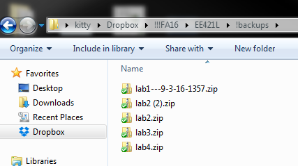
When finished backup your work (webpages and design
directory).
Return to Isaac's Labs
Return to EE 421L Labs