Lab 3 - ECE 421L
Authored
by Isaac Robinson,
robins82@unlv.nevada.edu
September 21st, 2016
This lab focuses on the layout of the 10-bit DAC designed and simulated in Lab 2.
- Use the n-well to layout a 10k resistor as discussed in Tutorial 1
- Discuss, in your lab
report, how to select the width and length of the resistor by
referencing the process information from MOSIS
The MOSIS scalable CMOS design rules implements a lambda of 300nm.
The mimimum width of n-well is 12 lambda:
300nm * 12 = 3.6 microns
Using this information we choose 4.5um as our width.
To determine our length:
R = (L * R[]) / W
thus
L = (R * W) / R[] = (10k * 4.5um) / (800) = 56.25um
But to allign the resistor to grid the value needs to be divisible by 0.15 microns.
4.5 / 0.15 = 30
56.25 / 0.15 = 375
(Note the tutorial used 56.1 [56.1 / 0.15 = 374] instead of 56.25 so this value is used in the lab)
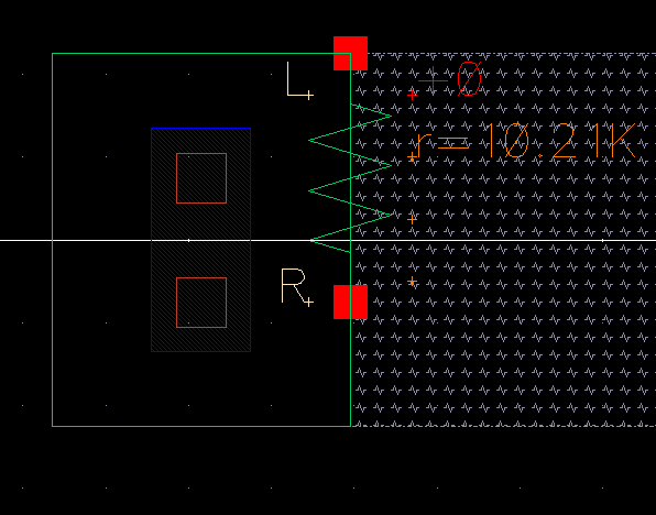
Image: The n-well resistor
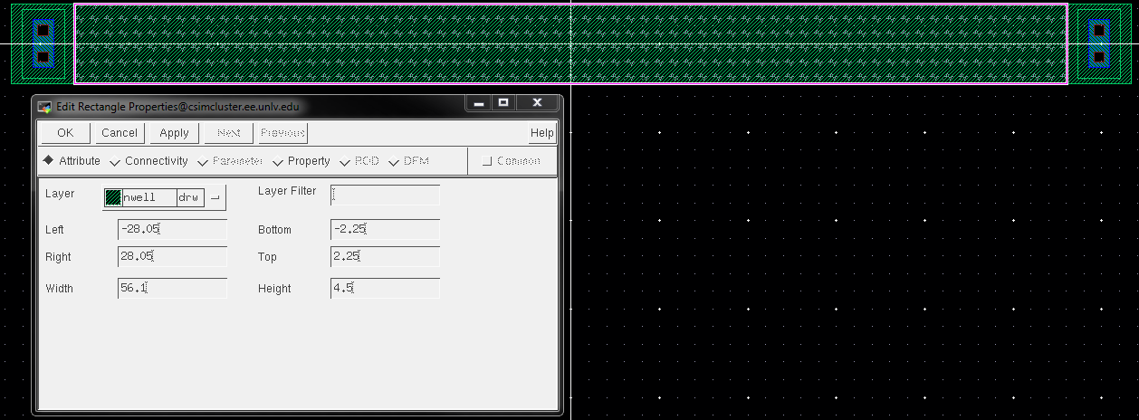
Image: The calculated value of resistance for the n-well resistor.
- Use this n-well
resistor in the layout of your DAC
- Discuss, in your lab
report, how the width and length of the resistor are measured
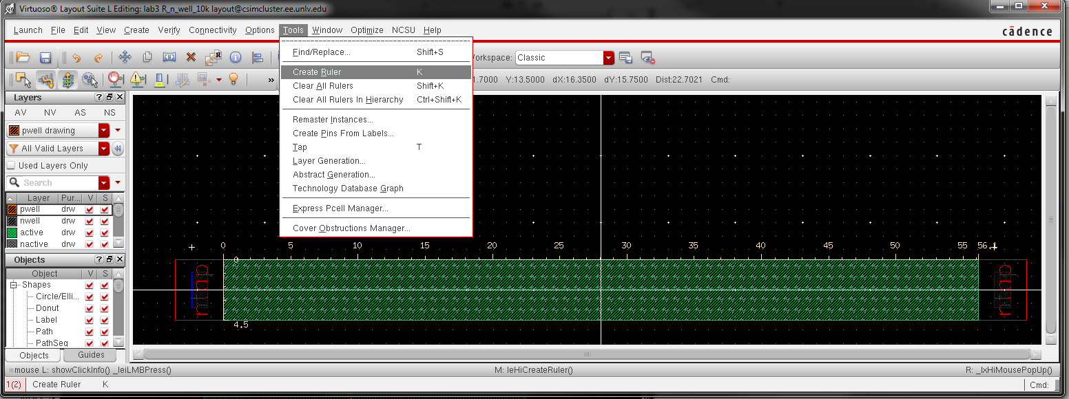
The width and length jof the resistor can be measured using the ruler tool in layout mode.
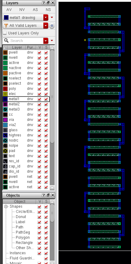
- Ensure that each
resistor in the DAC is laid out in parallel having the same x-position
but varying y-positions (the resistors are stacked)
- All input and output Pins should be on metal 1
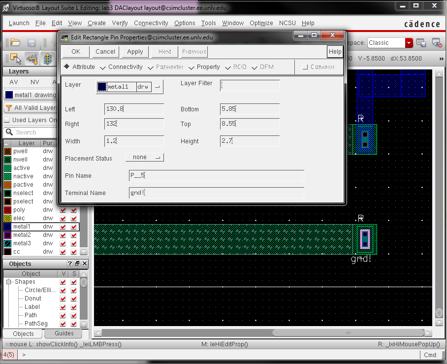
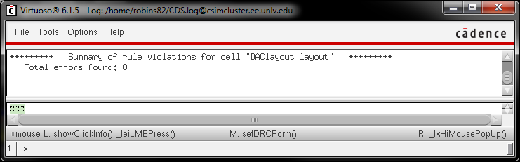
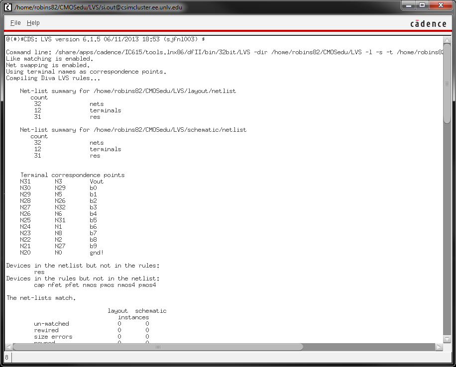
- DRC and LVS, with the extracted layout, your
design (show the results in your lab report)

- Zip up your final design directory and place it in the lab3 directory,
with a link on your lab report, so the grader can examine
both the layout and schematic (and simulations)
CLICK HERE for my final design directory.
Return to Isaac's Labs
Return to EE 421L Labs