Lab 6 - EE 421L 

Authored by Ja Manipon
maniponj@unlv.nevada.edu
10/26/16
Lab Files

Pre-Lab


Post-Lab


Drafting the Logic Gates


Inverter
NAND
XOR
Description
Schematic
http://cmosedu.com/jbaker/courses/ee421L/f16/students/maniponj/lab6/images/Inverter_Schematic.png
http://cmosedu.com/jbaker/courses/ee421L/f16/students/maniponj/lab6/images/NAND_Schematic.png
http://cmosedu.com/jbaker/courses/ee421L/f16/students/maniponj/lab6/images/XOR_Schematic.png
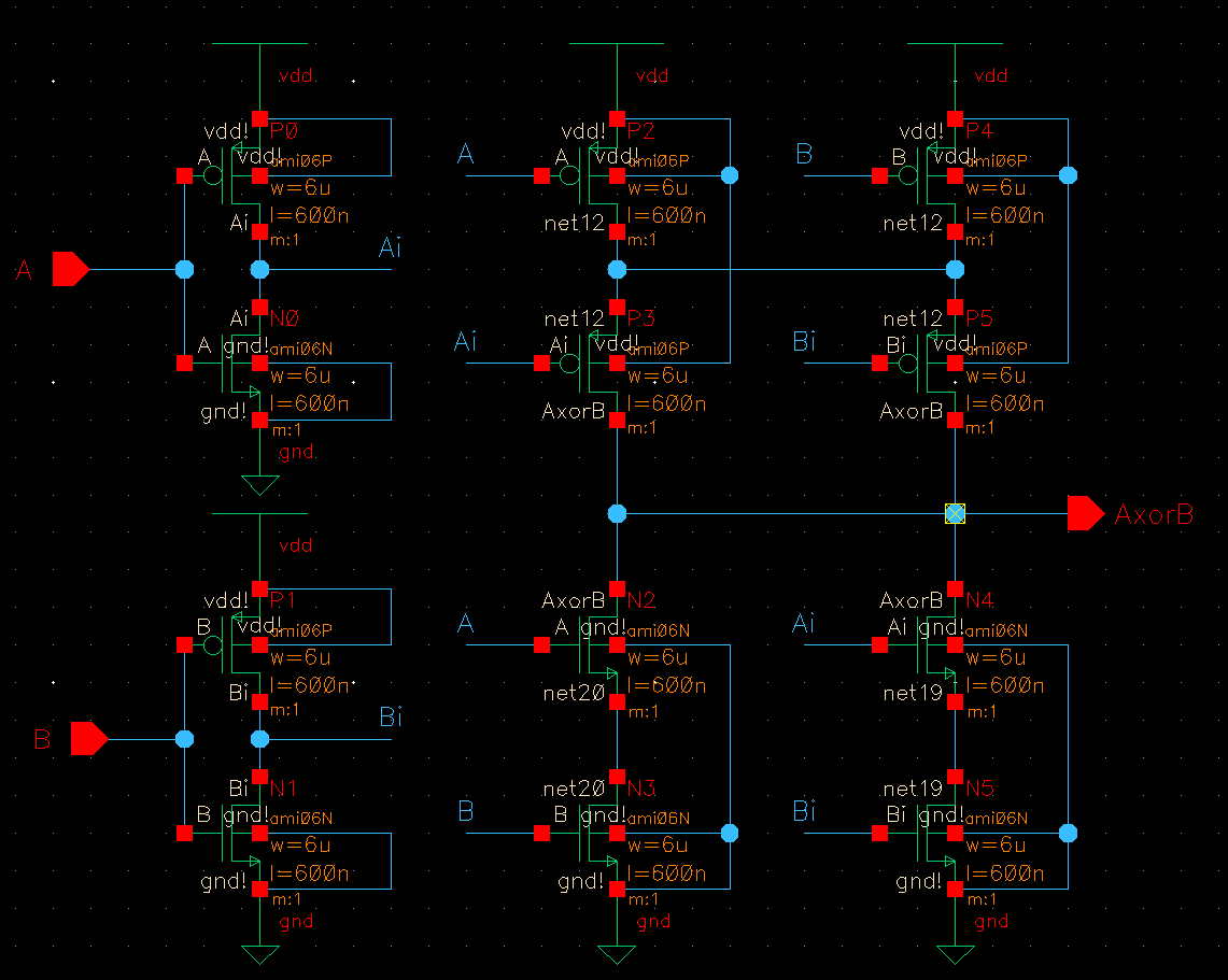
  • For each logic gate, I drafteted a schematic. The Inverter was already created because of the previous lab. The NAND and XOR gates were created based on the example images given in the Lab. The XOR actually used two sets of inverters.
Symbol
http://cmosedu.com/jbaker/courses/ee421L/f16/students/maniponj/lab6/images/Inverter_Symbol.png
http://cmosedu.com/jbaker/courses/ee421L/f16/students/maniponj/lab6/images/NAND_Symbol.png
http://cmosedu.com/jbaker/courses/ee421L/f16/students/maniponj/lab6/images/XOR_Symbol.png
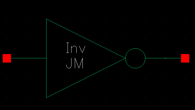
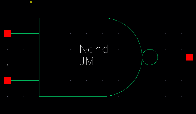
  • After I checked and saved each schematic, I drew the symbol to the common logic gate symbol respectively
Layout
http://cmosedu.com/jbaker/courses/ee421L/f16/students/maniponj/lab6/images/Inverter_Layout.png
http://cmosedu.com/jbaker/courses/ee421L/f16/students/maniponj/lab6/images/NAND_Layout.png
http://cmosedu.com/jbaker/courses/ee421L/f16/students/maniponj/lab6/images/XOR_Layout.png
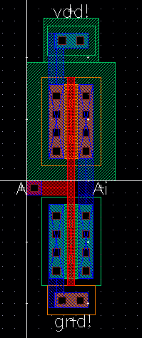
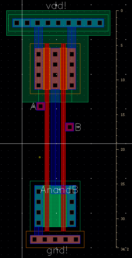
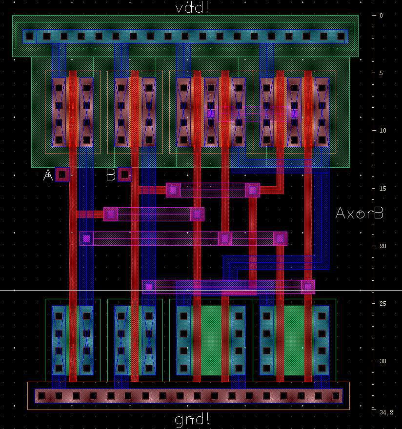
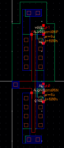
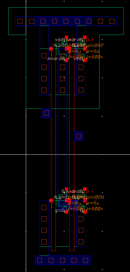
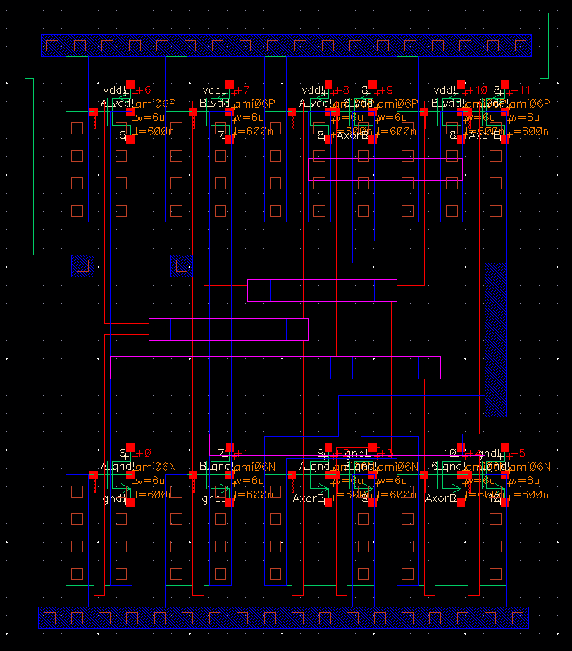
  • Next, I layed out each of the schematics. The inverter was already made from the previous lab. The NAND gate could be drawn with a single NMOS and PMOS but with a multiplier of 2. The XOR used a similar technique of the NAND and two inverters were also added to the layout for the first half of the schematic.The Ruler that is on both the NAND and XOR were used to help line up the logic gates for the final Full Adder layout.
DRC
http://cmosedu.com/jbaker/courses/ee421L/f16/students/maniponj/lab6/images/Inverter_DRC.png
http://cmosedu.com/jbaker/courses/ee421L/f16/students/maniponj/lab6/images/NAND_DRC.png
http://cmosedu.com/jbaker/courses/ee421L/f16/students/maniponj/lab6/images/XOR_DRC.png
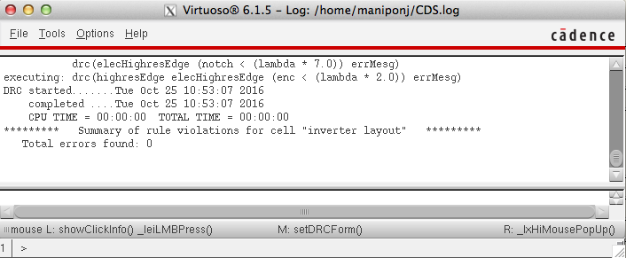
  • All of the layouts DRC'd without any issue.
Extracted http://cmosedu.com/jbaker/courses/ee421L/f16/students/maniponj/lab6/images/Inverter_Extracted.png
http://cmosedu.com/jbaker/courses/ee421L/f16/students/maniponj/lab6/images/NAND_Extracted.png
http://cmosedu.com/jbaker/courses/ee421L/f16/students/maniponj/lab6/images/XOR_Extracted.png
  • Here all of the extracted views of each of the logic gates.
LVS
http://cmosedu.com/jbaker/courses/ee421L/f16/students/maniponj/lab6/images/Inverter_LVS.png
http://cmosedu.com/jbaker/courses/ee421L/f16/students/maniponj/lab6/images/NAND_LVS.png
http://cmosedu.com/jbaker/courses/ee421L/f16/students/maniponj/lab6/images/XOR_LVS.png
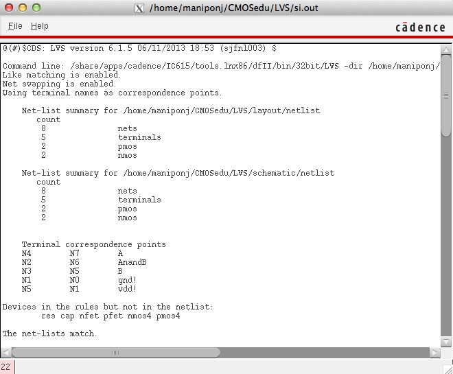
  • After I extracted all the layouts, I ran the LVS and all the netlists matched.


Simulation of the Logic Gates

Schematic
http://cmosedu.com/jbaker/courses/ee421L/f16/students/maniponj/lab6/images/Sim_Gates_Schematic.png
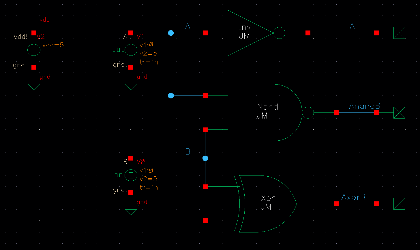
  • Once I finished drafting all the logic gates, I began the setup for the schematic for simulations. In this schematic, I have connected each of the logic gate to either one or two inputs. I also have added a VDD! source to power all the gates for NMOS and PMOS. The inputs going in are pulse waves simulating a binary counter going from 0 to 3. Since there is only at most two inputs, all combinations needed are four combinations.
Simulation
http://cmosedu.com/jbaker/courses/ee421L/f16/students/maniponj/lab6/images/Sim_Gates_Simulation.png

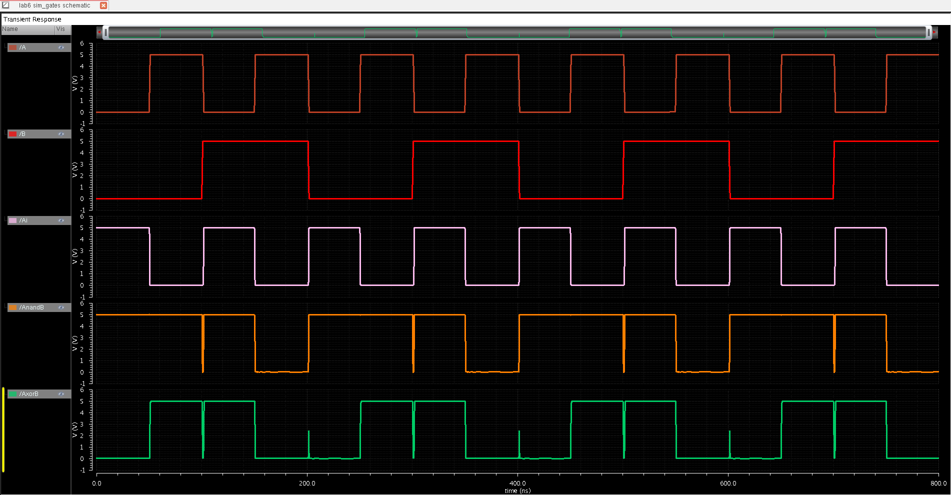
  • Here are the results of our simulation. From the chart, the inputs are going through 00, 01, 10, and 11 and all the gates are outputting correctly as shown in the truth table below. In addition to the schematic simulation, an extracted simulation was ran as well showing that too is functioning correctly.
  • Glitches: Another observation to the simulation is that there are glitches occuring either the rising edge or falling edge of the inputs. This occurs because an input is transitioning and in that time frame may be considered on or off and the logic gate will output  what it currently sees in that transition until it reaches a steady state.
Truth Table
Input
Output
A
B
Ai
AnandB
AxorB
0
0
1
1
0
0
1
1
1
1
1
0
0
1
1
1
1
0
0
0

Extracted Simulation/Netlist
http://cmosedu.com/jbaker/courses/ee421L/f16/students/maniponj/lab6/images/Sim_Gates_ExtractedSimulation.png
http://cmosedu.com/jbaker/courses/ee421L/f16/students/maniponj/lab6/images/Sim_Gates_Netlist.png


Drafting the Full Adder

Schematic
http://cmosedu.com/jbaker/courses/ee421L/f16/students/maniponj/lab6/images/FullAdder_Schematic.png
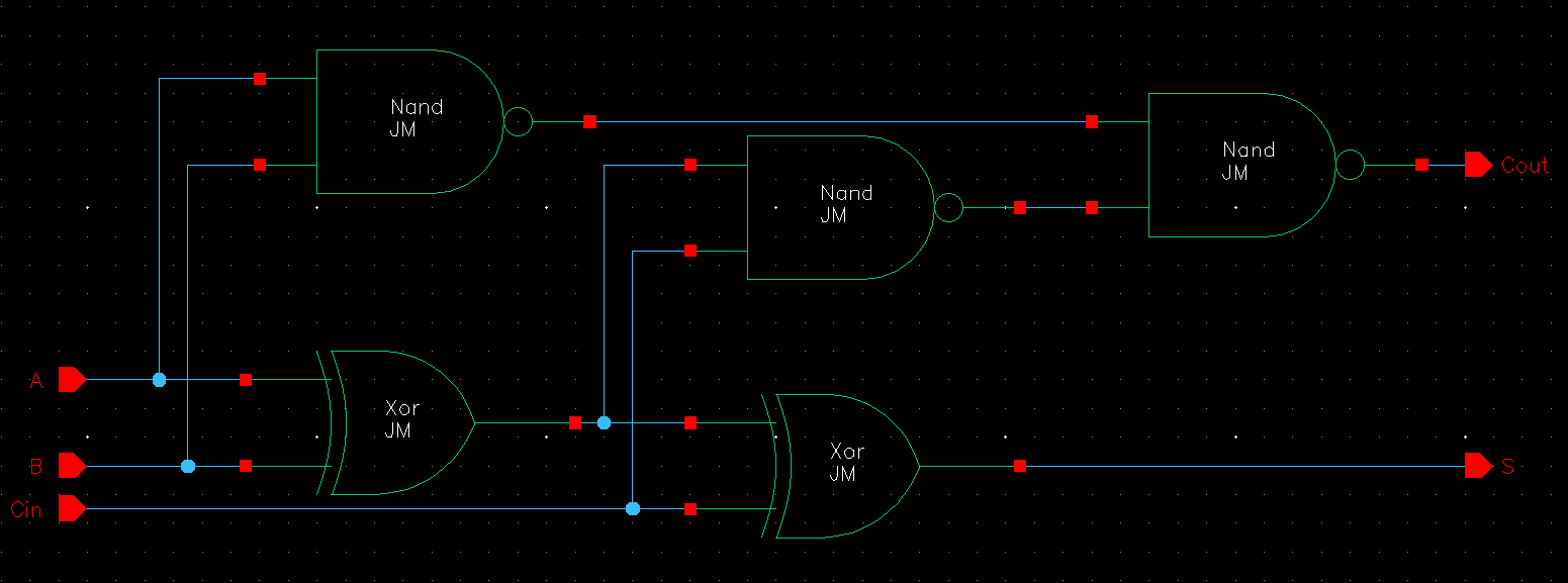
  • After all the gates have been simulated and verified outputting correctly, I began drafting the Full Adder in schematic view. This was based on the Full Adder schematic example. The Full Adder is a common logic design. This specific Full Adder is a 1-bit Full Adder. It has three inputs and two outputs. The inputs are A, B and Carry In and the outputs are Sum and Carry Out. This Full Adder takes in three 1-Bit inputs and add them together producing a sum and that sum is split between an S and Cout. The gates that are used are the ones I drafted and simulated earlier in this lab.
Symbol
http://cmosedu.com/jbaker/courses/ee421L/f16/students/maniponj/lab6/images/FullAdder_Symbol.png
  • The next step, was to create a symbol for simulations later on and the symbol to the left is the common 1-bit Full Adder symbol.
Layout
http://cmosedu.com/jbaker/courses/ee421L/f16/students/maniponj/lab6/images/FullAdder_Layout.png
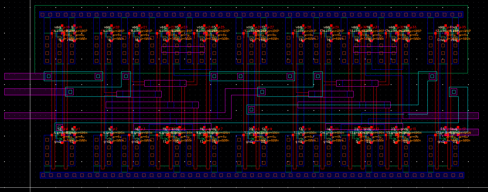
  • Next, I began laying out the Full Adder. I used the layouts of the of the gates previously made and everything lined up thanks to the ruler measurements made earlier. I connected all the gates according to the schematic made earlier. With this designed, I tried to keep all the wires in between all the PMOS's and NMOS's. All of the metal1 wires connected the sources and draines that needed to be connected, metal2 connected all the gates and metal 3 connected all the logic gates together. After everything was connected I flattened the logic gates in order to have one long row of ntap and ptap for the vdd and ground. I also added all the pins needed; vdd!, gnd!, A, B, Cin, S, Cout.The white outlines in this final layout show the individual logic gates for clarity.
DRC
http://cmosedu.com/jbaker/courses/ee421L/f16/students/maniponj/lab6/images/FullAdder_DRC.png
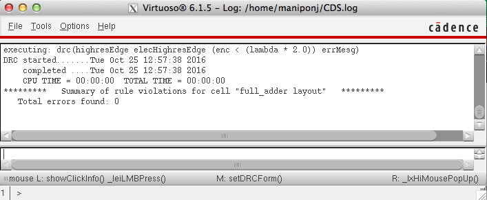
  • I ran the DRC to make sure all of the cells were not violating any rules and there were no errors
Extracted
http://cmosedu.com/jbaker/courses/ee421L/f16/students/maniponj/lab6/images/FullAdder_Extracted.png
  • After DRC, I extracted the layout so I can run the LVS
LVS
http://cmosedu.com/jbaker/courses/ee421L/f16/students/maniponj/lab6/images/FullAdder_LVS.png
  • I ran the LVS and netlists matched.


Simulation of Full Adder

Schematic
http://cmosedu.com/jbaker/courses/ee421L/f16/students/maniponj/lab6/images/Sim_FullAdder_Schematic.png
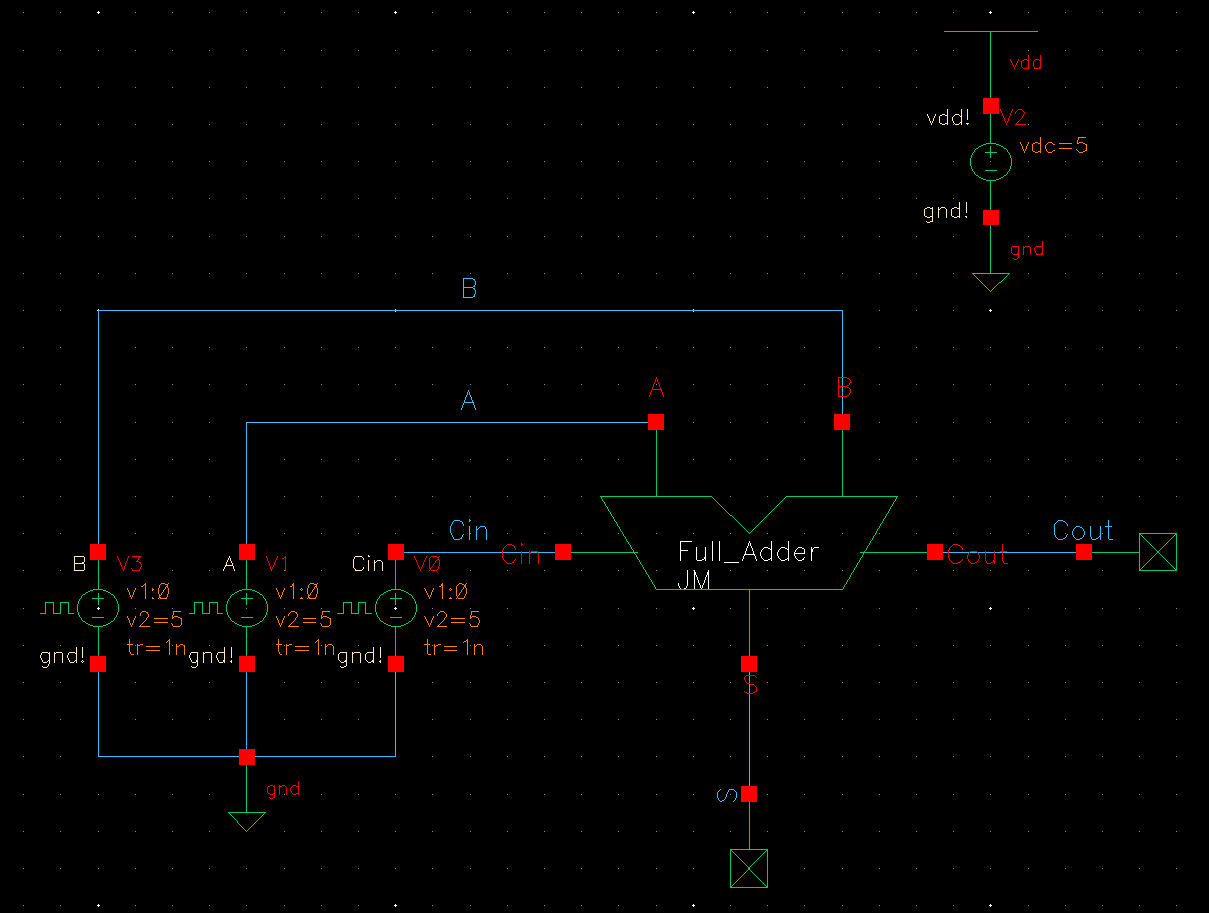
  • Once I finished the layout, I began drafting the schematic needed to simulate both the schematic view and the layout view of the Full Adder.
Simulation
http://cmosedu.com/jbaker/courses/ee421L/f16/students/maniponj/lab6/images/Sim_FullAdder_Simulation.png


  • After running the simulation, we can see the Full Adder is working perfectly according to the truth table below for both the extracted and schematic view. Similar to the previous simulation there are glitches as well when the inputs are transitioning.
Truth Table
Input
Output
A
B
Cin
S
Cout
0
0
0
0
0
0
0
1
1
0
0
1
0
1
0
0
1
1
0
1
1
0
0
1
0
1
0
1
0
1
1
1
0
0
1
1
1
1
1
1

Extracted Simulation/Netlist
http://cmosedu.com/jbaker/courses/ee421L/f16/students/maniponj/lab6/images/Sim_FullAdder_ExtractedSimulation.png
http://cmosedu.com/jbaker/courses/ee421L/f16/students/maniponj/lab6/images/Sim_FullAdder_Netlist.png

Return to EE 421 Labs