Lab 4 - ECE 421L
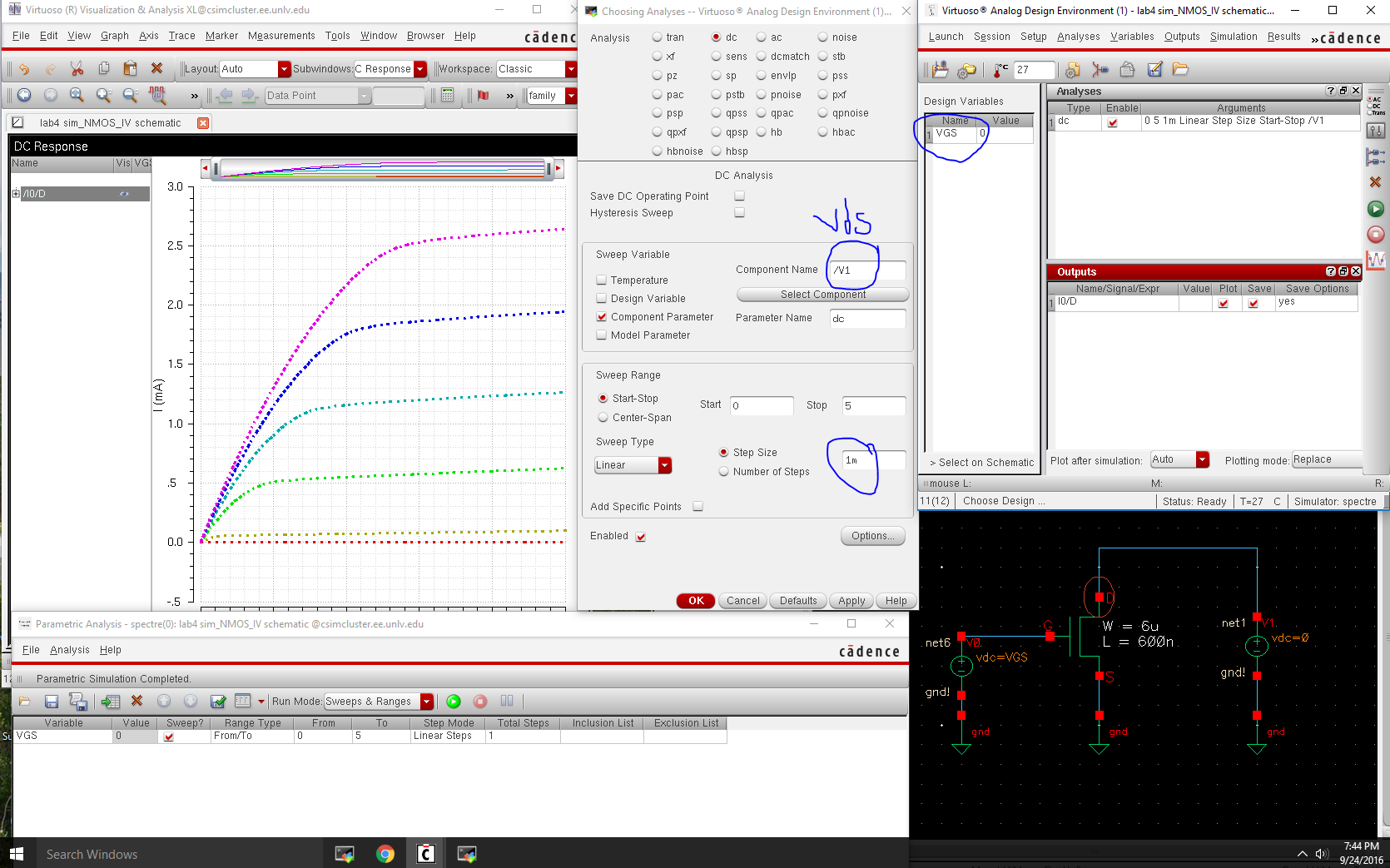
a). A schematic for simulating ID v. VDS of an NMOS device for VGS varying from 0 to 5 V in 1 V steps while VDS varies from 0 to 5 V in 1 mV steps. Use a 6u/600n width-to-length ratio.
schematic and waveform:
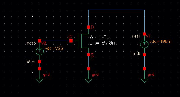
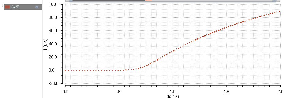
b). A schematic for simulating ID v. VGS of an NMOS device for VDS = 100 mV where VGS varies from 0 to 2 V in 1 mV steps. Again use a 6u/600n width-to-length ratio.
Schematic and waveform:
c).
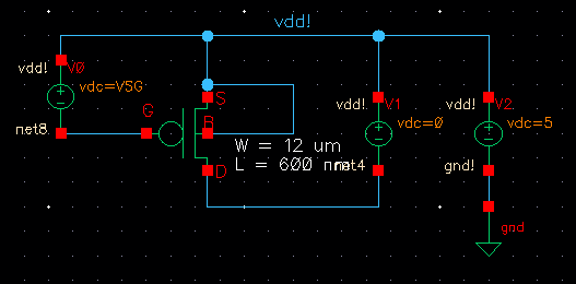
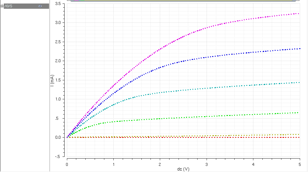
A schematic for simulating ID v. VSD (note VSD not VDS) of a PMOS
device for VSG (not VGS) varying from 0 to 5 V in 1 V steps while VSD
varies from 0 to 5 V in 1 mV steps. Use a 12u/600n width-to-length ratio.
Schematic and waveform:
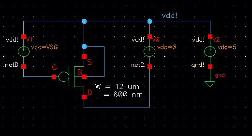
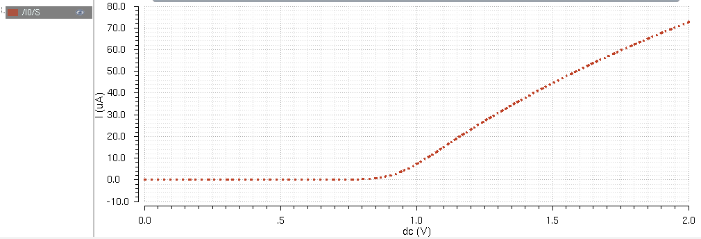
d). A schematic for simulating ID v. VSG of a PMOS device for VSD = 100 mV where VSG varies from 0 to 2 V in 1 mV steps. Again, use a 12u/600n width-to-length ratio.
schematic and simulation:
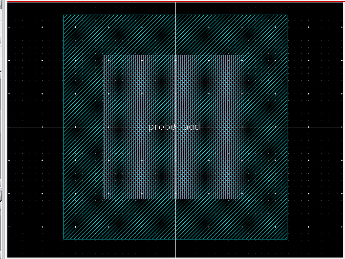
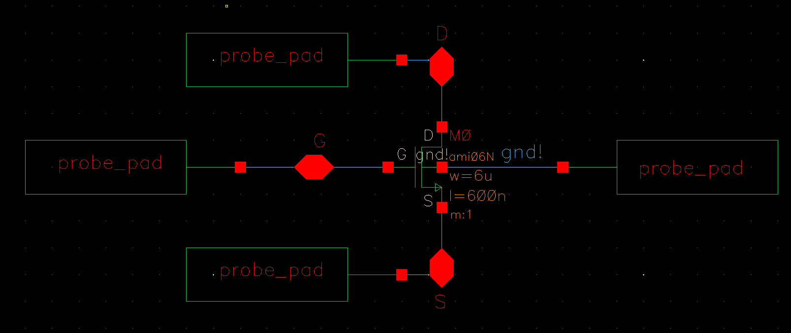
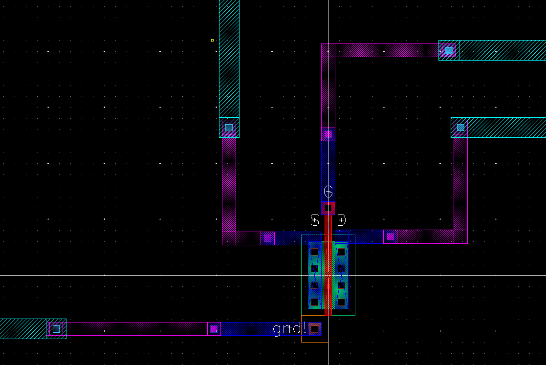
2). Lay out a 6u/0.6u NMOS device and connect all 4 MOSFET terminals to probe pads.
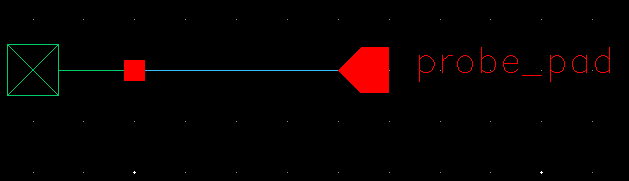
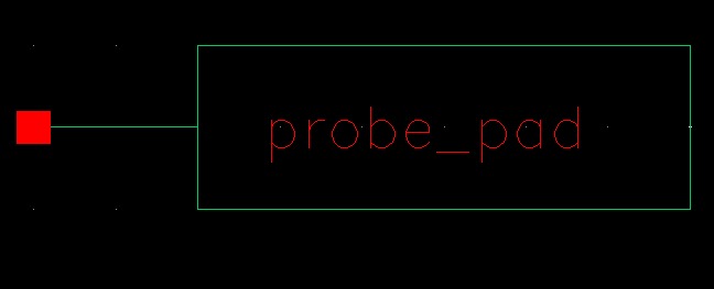
3). Lay out a 12u/0.6u PMOS device and connect all 4 MOSFET terminals to probe pads.
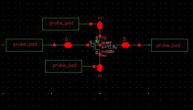
PMOS Schematic:
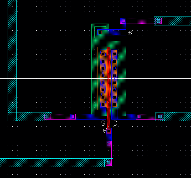
PMOS Layout:
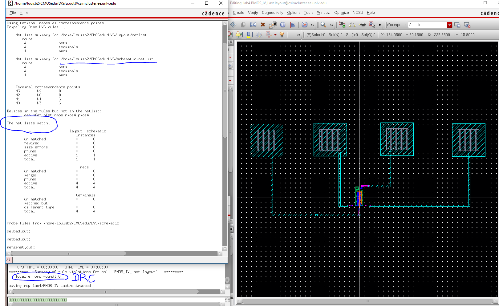
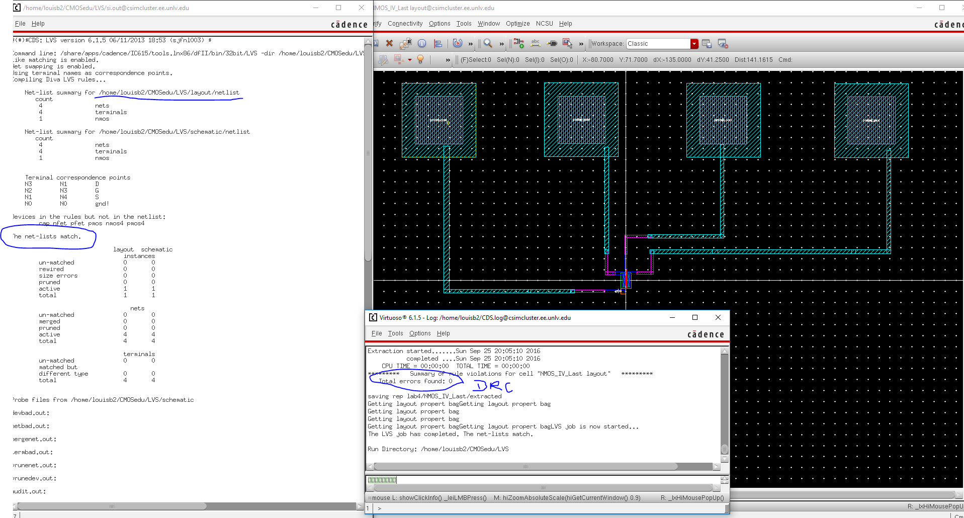
PMOS LVS & DRC check + connected pads: