Lab 3 - ECE 421L 

Authored by Billy J. Louis III,

Email: Louisb2@unlv.nevada.edu

Today's date: 20 September 2016


Lab description: Lab3 - Layout of a 10-bit DAC, due September 21 

This lab will focus on the layout of the 10-bit DAC you designed and simulated in Lab 2


BackUp File:

As it is said in the first lab, I do not use online back up for any of my acedemic works.  I save everything

on my computer and back up my computer using a hardrive., I do so, once a month.

http://cmosedu.com/jbaker/courses/ee421L/f16/students/louisb2/lab3/3_backUpPicture.PNG
   

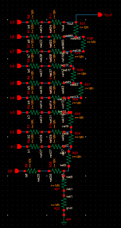
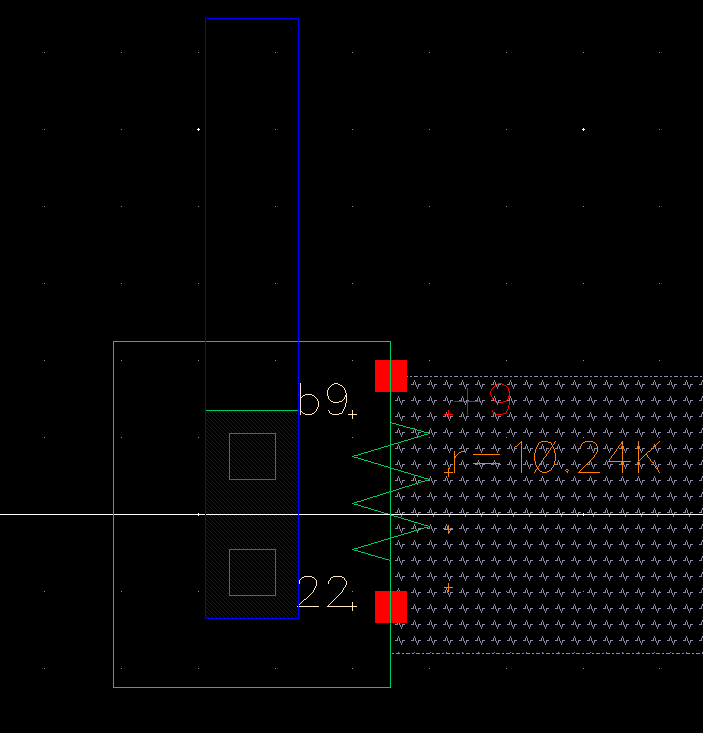
This lab is a continuity of LAB2 in which I have designed a DAC using 10k resistors:
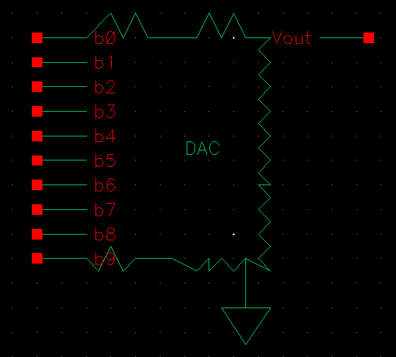
Shematic & Symbol:

http://cmosedu.com/jbaker/courses/ee421L/f16/students/louisb2/lab3/0_1_Schematic.PNG  http://cmosedu.com/jbaker/courses/ee421L/f16/students/louisb2/lab3/0_2_Symbol.PNG


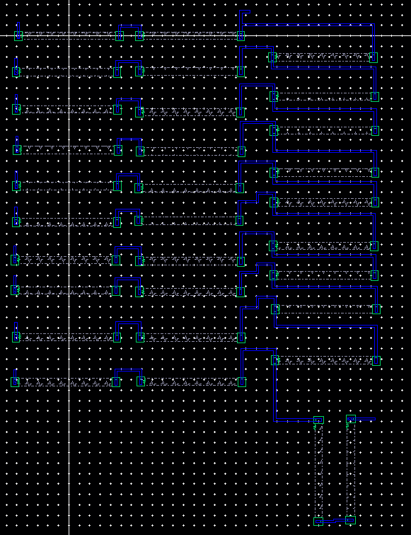
The Following images will be attributed only to the layout of the DAC

In order to design the 10k resistor before instantiating it one has to

find the appropriate parameters,

with Rsquare = 800 Ohms/square the length and the width of a 10k 

resistor would be:

10k = 800 * (L/W) with W = 3.6, we have L = 45.

http://cmosedu.com/jbaker/courses/ee421L/f16/students/louisb2/lab3/2_extractedPin9.PNG


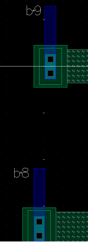
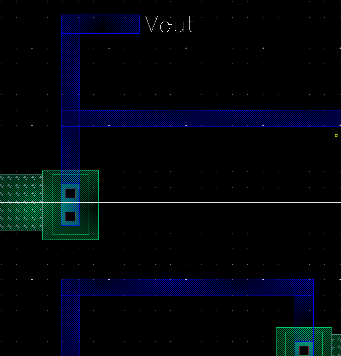
Images of INPUT PIN b9 - b8 - and OUTPUT PIN Vout:

http://cmosedu.com/jbaker/courses/ee421L/f16/students/louisb2/lab3/1Layout2Pins.PNG http://cmosedu.com/jbaker/courses/ee421L/f16/students/louisb2/lab3/1Layout3Pins.PNG


Layout & extracted DAC:

http://cmosedu.com/jbaker/courses/ee421L/f16/students/louisb2/lab3/1Layout1.PNG


http://cmosedu.com/jbaker/courses/ee421L/f16/students/louisb2/lab3/2_extracted.PNG

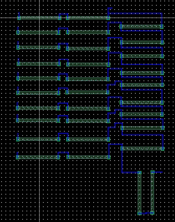
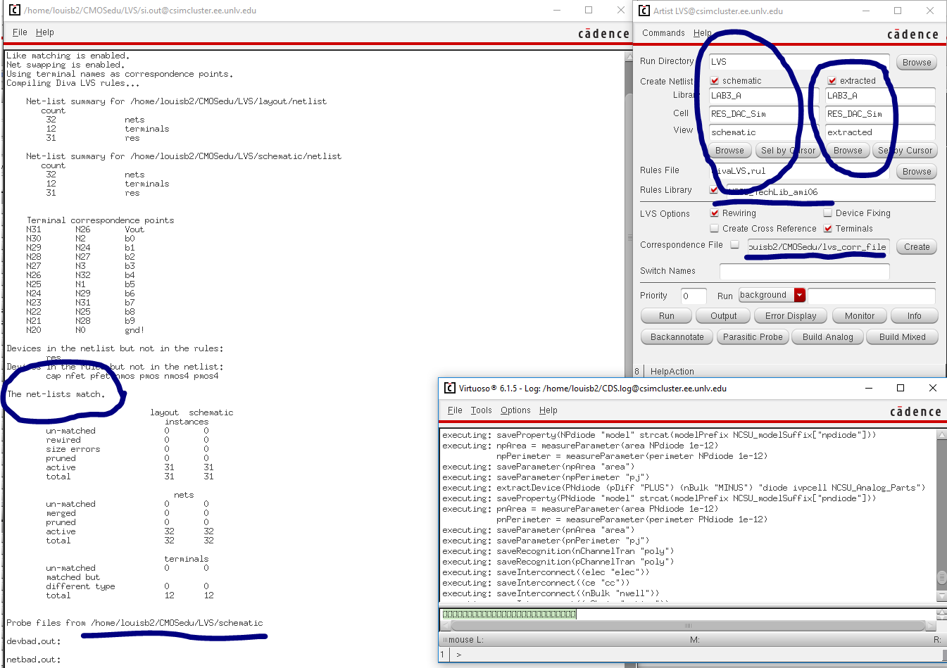
After completion of the layout & the extracted DAC, the design pass the LVS check:

http://cmosedu.com/jbaker/courses/ee421L/f16/students/louisb2/lab3/1_LVS_check.PNG


The END - Return To EE 421 L