Lab 2 - ECE 421L
Authored
by Billy J. Louis III,
Today's
date
7 September 2016
Lab
description: Analog to Digital Converter
PreLab2
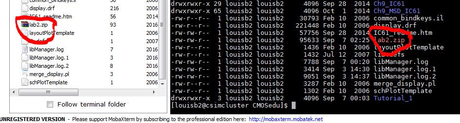
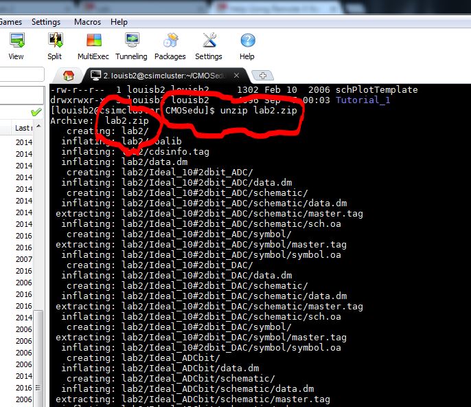
Unzipped file
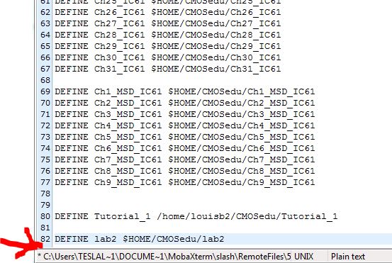
Library Update:
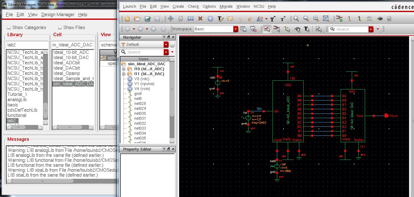
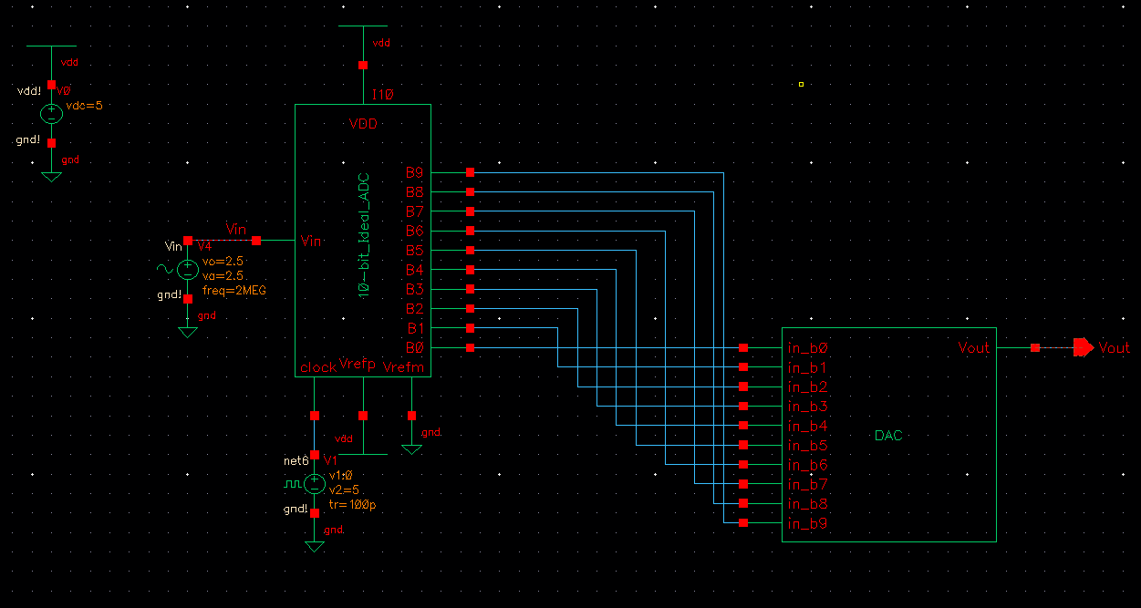
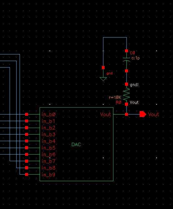
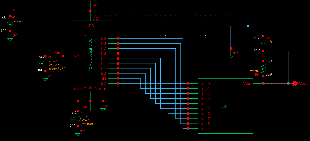
Schematic:
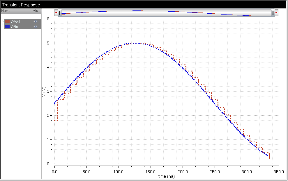
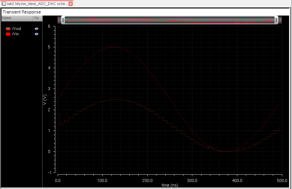
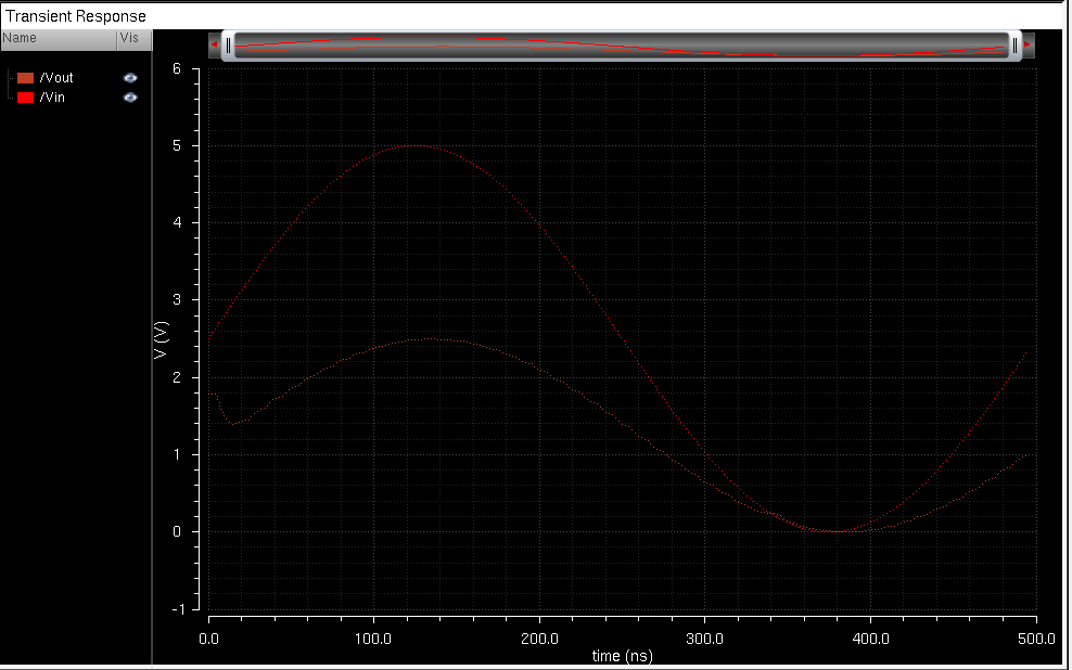
Waveform1 (normal backGround):
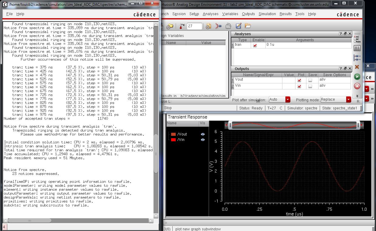
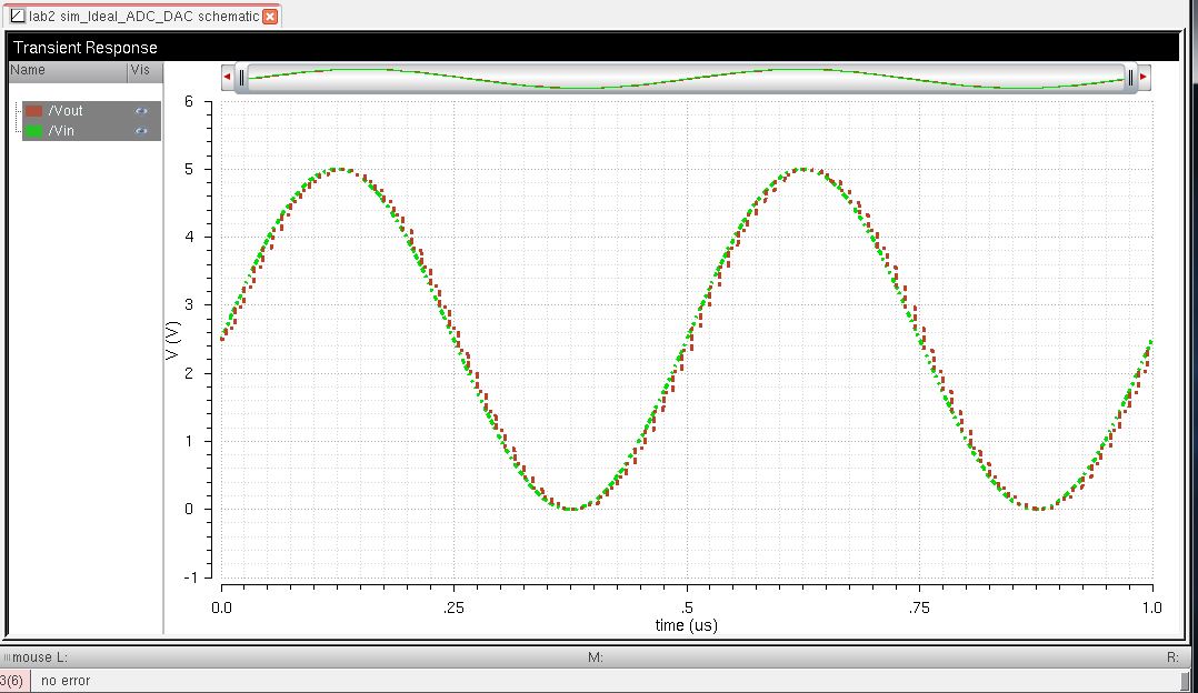
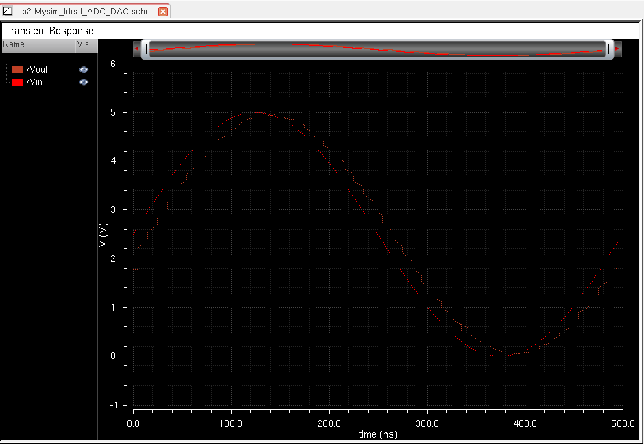
Waveform (changed backGround):
REMARK:
As long as the input signal is greater than zero and less than VDD the output signal will be correct.
------------------------------------------------------------------------------------------------------------------------------------------------------------
RETURN TO EE421L
------------------------------------------------------------------------------------------------------------------------------------------------------------
POSTLAB STARTS HERE:
Description: Lab Report
Today's date: 14 September 2016
1)- 10-Bit DAC using 10K resistors:
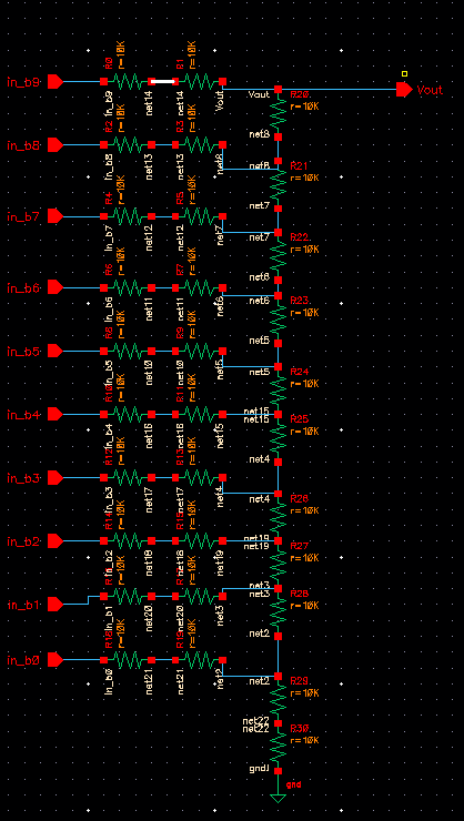
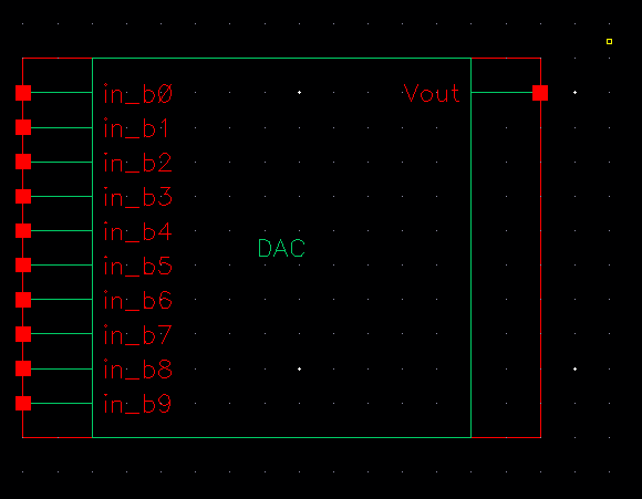
Schematic & waveform for the designed and tested DAC:
2)- How to determine the output resistance of the DAC (answer: R) by combining resistors in parallel and series
ANSWER:
Starting with (R_30 + R_29) || (R_19 + R_18) = 2R || 2R =R and R + R = 2R
Then, when taking R_28 and R_16 + R_17 we have 2R || 2R = R and R + R = 2R
Taking this pattern untill reaching R_20 and R_0 + R_1 = 2R || 2R = R
Where the output resistance Rout = R
3)- Delay Driving a Load:
a. Ground all DAC inputs except B9
Hand Calculation:
Time delay = Td = 0.7RC = 0.7 * 10k * pF = 0.070 * [10^[-6]] = 70ns
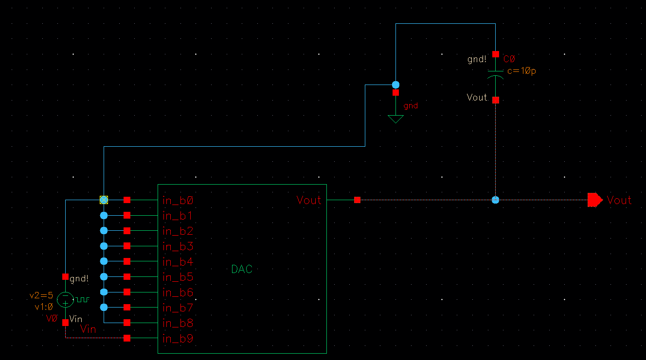
4) - Final Design with no load (schematic & simulation):
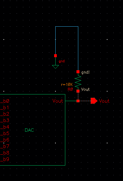
Load with a 10K Resistor:
Load with a 10K resistor and a 1pF capacitor:
Load with a 10K resistor in parallel with 1pF capacitor:
The End: Return To EE421L