Lab 8 - EE 421L
Authored by:
Dominique
Anguiano - anguian3@unlv.nevada.edu
Michael
Ghisilieri - ghisilie@unlv.nevada.edu
Martin
Jaime - jaimem5@unlv.nevada.edu
Billy
Louis - louisb2@unlv.nevada.edu
October
26, 2016
Lab
chip for this project: Chip6_f16
Chip Devices
The
chip contains the following devices
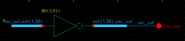
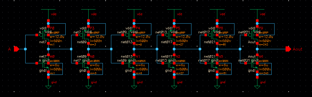
- A 31-stage ring oscillator with a buffer for driving a 20 pF off-chip load
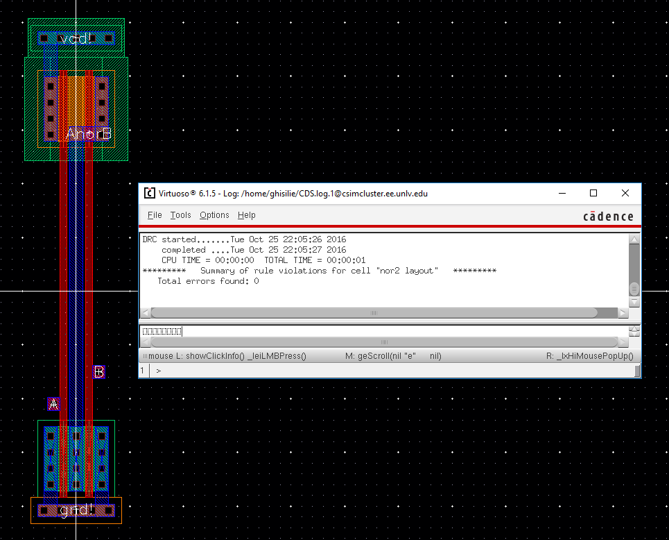
- NAND and NOR gates using 6/0.6 NMOSs and PMOSs
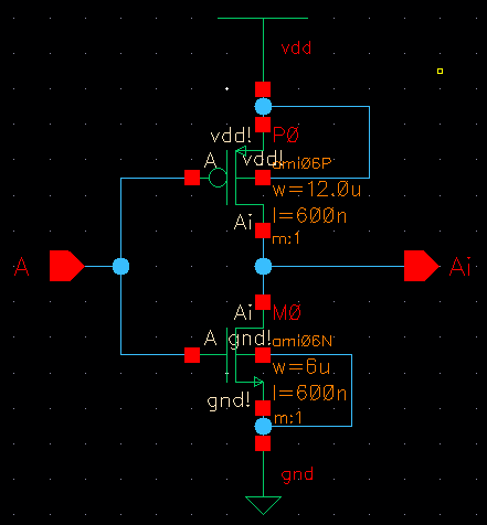
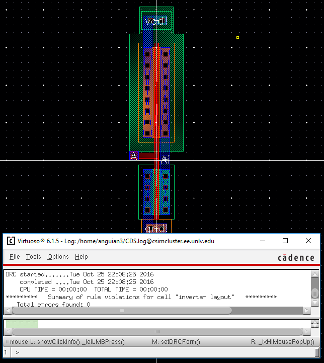
- An inverter made with a 6/0.6 NMOS and a 12/0.6 PMOS
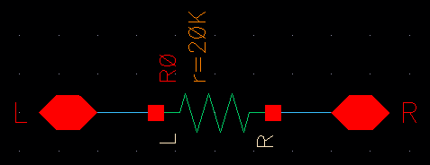
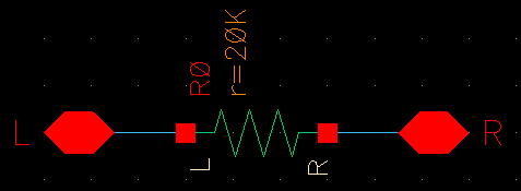
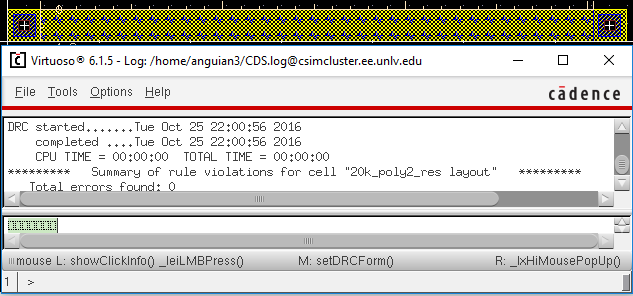
- 20k resistors, one made using n-well and the other using hi-res poly2
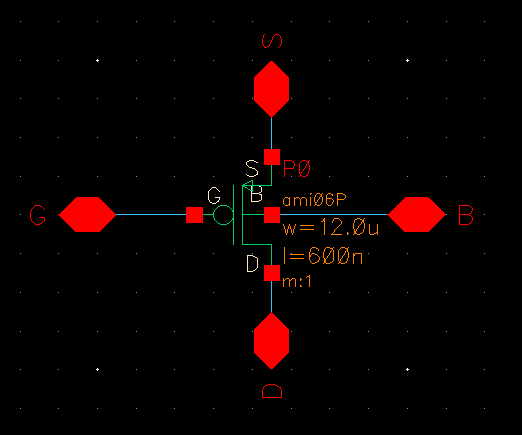
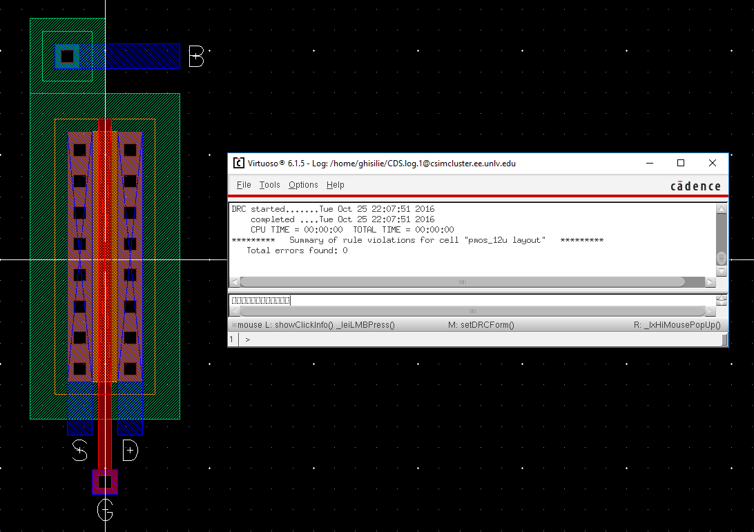
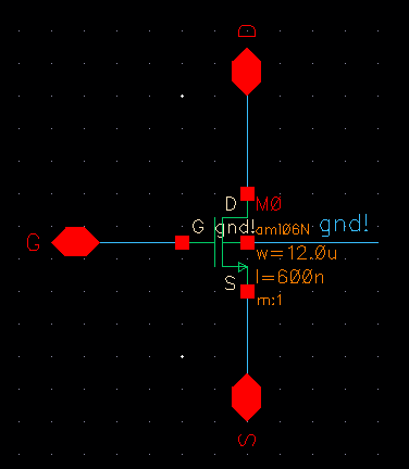
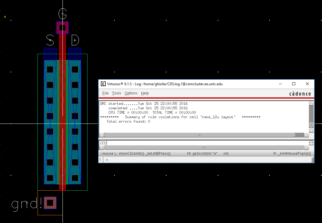
- 12u/0.6u PMOS and NMOS devices
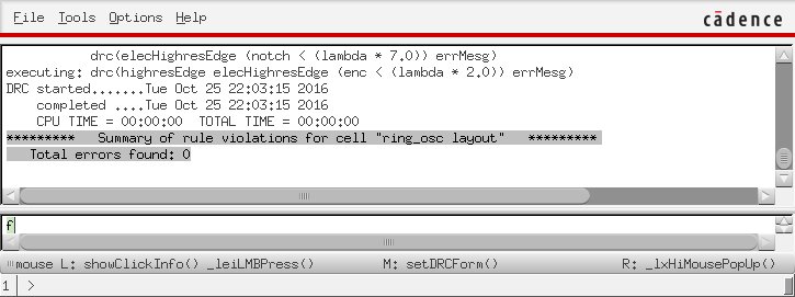
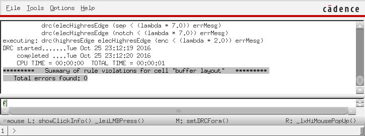
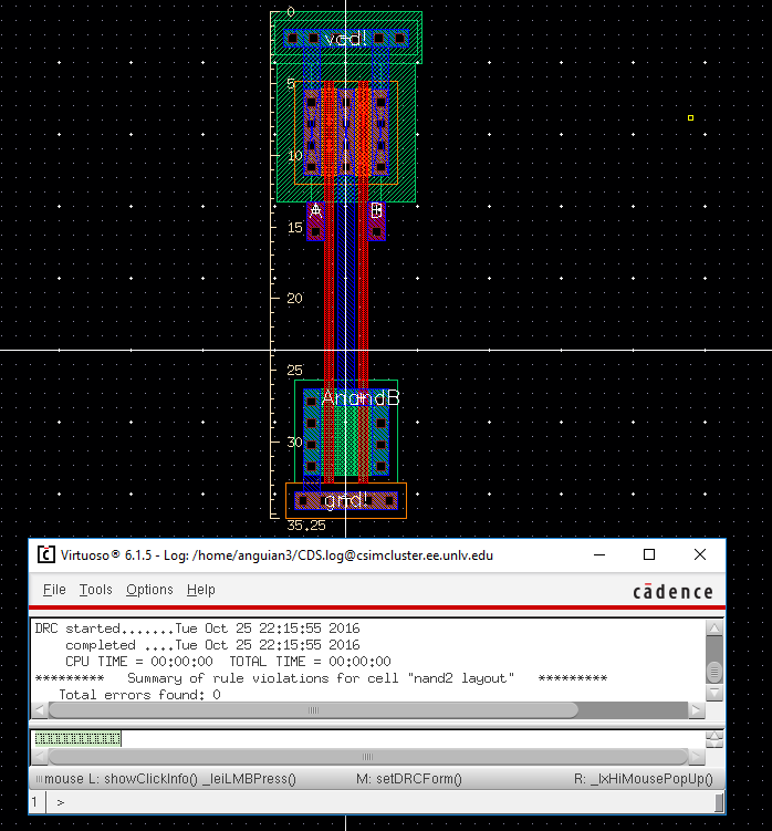
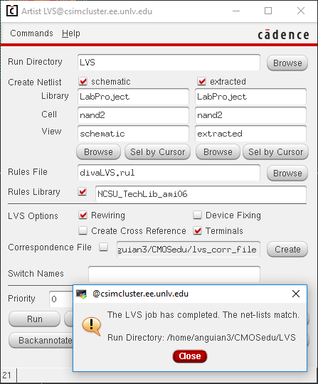
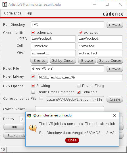
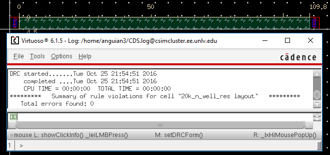
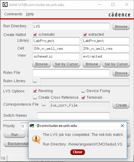
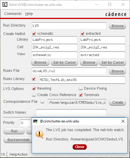
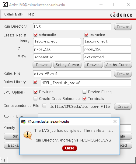
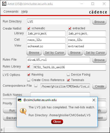
Schematic, DRC, and LVS of each device
A 31-stage ring oscillator (top) with a buffer (bottom) for driving a 20pF off-chip load
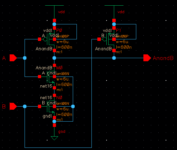
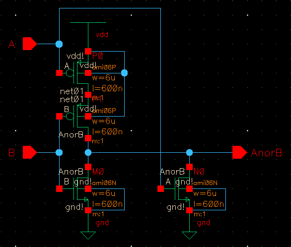
NAND (top) and NOR (bottom) gates using 6/0.6 NMOSs and PMOSs
An inverter made with a 6/0.6 NMOS and a 12/0.6 PMOS
20k resistors, one made using n-well (top) and the other using hi-res poly2 (bottom)
12u/0.6u PMOS (top) and NMOS (bottom) devices
Schematic and layout of padframe
Pin Chart
Return to EE421L Labs