Lab Project - EE 421L
deignank@unlv.nevada.edu
Design a
circuit that takes a serial input and detects (outputs a high logic signal called
detect) the sequence 101011. The inputs to your circuit are clk and in. Make
sure that the output of your design, detect, is buffered before connecting to a
pad.
Components Needed:
-D Flip-Flop
-transmission gates
-inverters
-6-bit AND
gate
-Buffer for
the output
Design of D Flip-Flop:
The first step
in creating a D Flip-Flop is to create a transmission gate. A transmission gate
consists of a PMOS and NMOS connected by the drain and sources. Both devices
are used so that full logic levels can be passed (NMOS passes low well and PMOS
passes high well). When both the transistors are on, the input is passed
through the gate. Below is my schematic and symbol for the transmission gate:
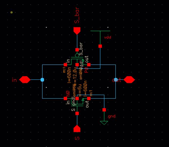
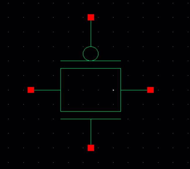
As shown
above, I chose the PMOS to be twice as wide as the NMOS. This is because
electron mobility is higher than hole mobility. This assures for approximately
equal fall and rise times.
The other
component needed for a D flip flop is an iverter, which was already designed in
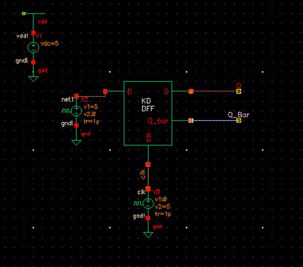
lab. Below is the full schematic for my D flip flop:
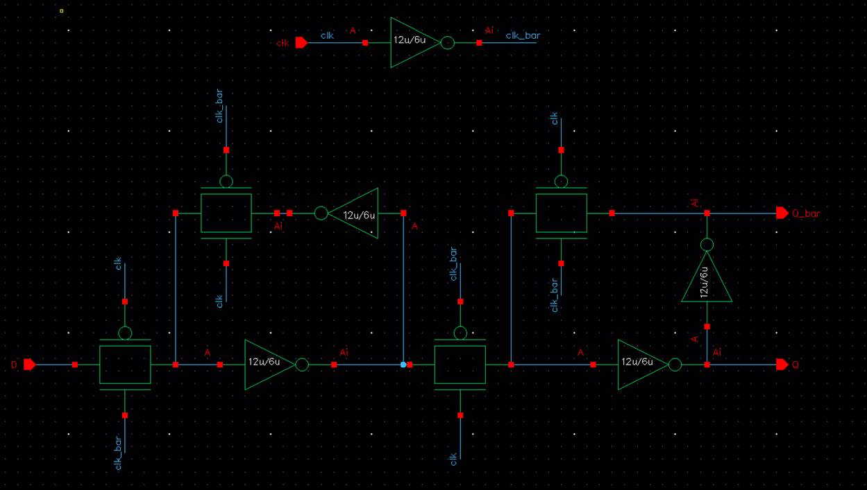
As seen above,
clk_bar was produced within the circuit so the only 4 pins are clk, D, Q, and Q
bar. I created a symbol for the above schematic shown below:
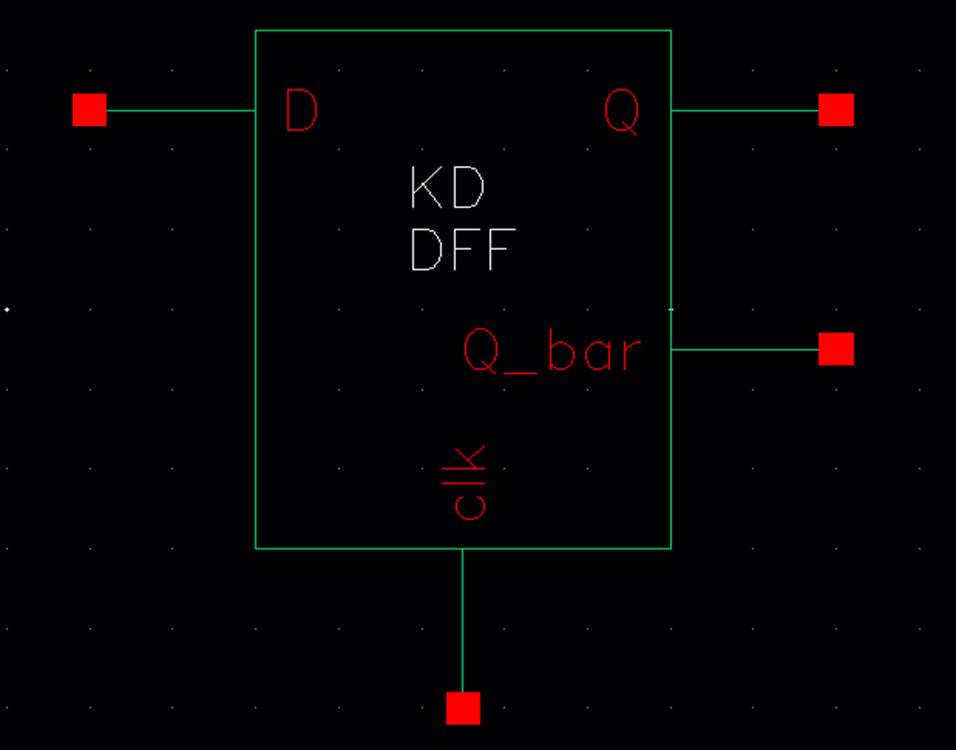
The above
symbol was used to simulate the operation of the D flip-flop. The input from D
is passed to Q on every rising edge of the clock. Cascaded flip flops are
needed to provide memory for the detector circuit to read serial inputs. Below
shows the successful operation of the flip-flop:
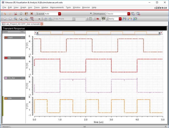
The
waveform shows the output, Q and Q bar, taking the same logic level as D on the
rising edge.
6-Bit AND
Gate:
I was able to
extend a 2-bit AND gate to 6-bit by connecting 4 gates together. Below is the
schematic a 2-bit AND gate and 6-bit gate:
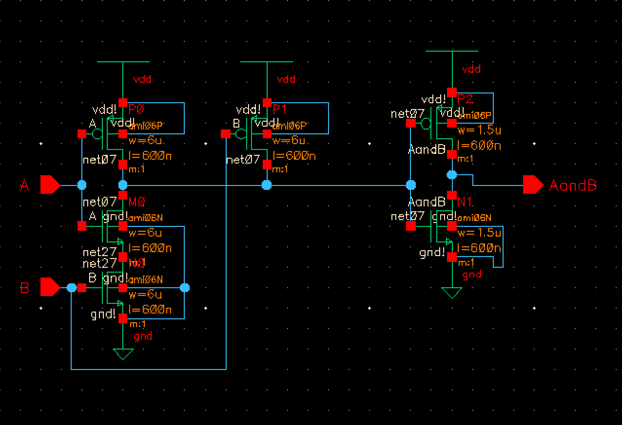
When both A
and B are high, the input to the inverter will be pulled to ground, causing the
output to go high. All other cases result in a 0 at the output.

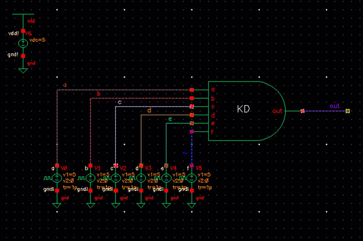
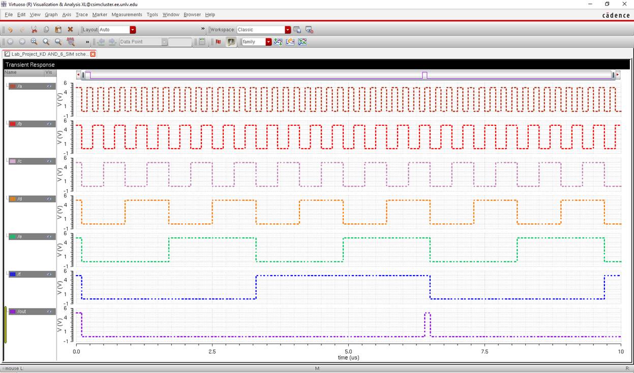
I created a
symbol from the above schematic and simulated its operation. As shown below,
the output is only high when all the inputs are high. The output is the bottom
line shown in purple.
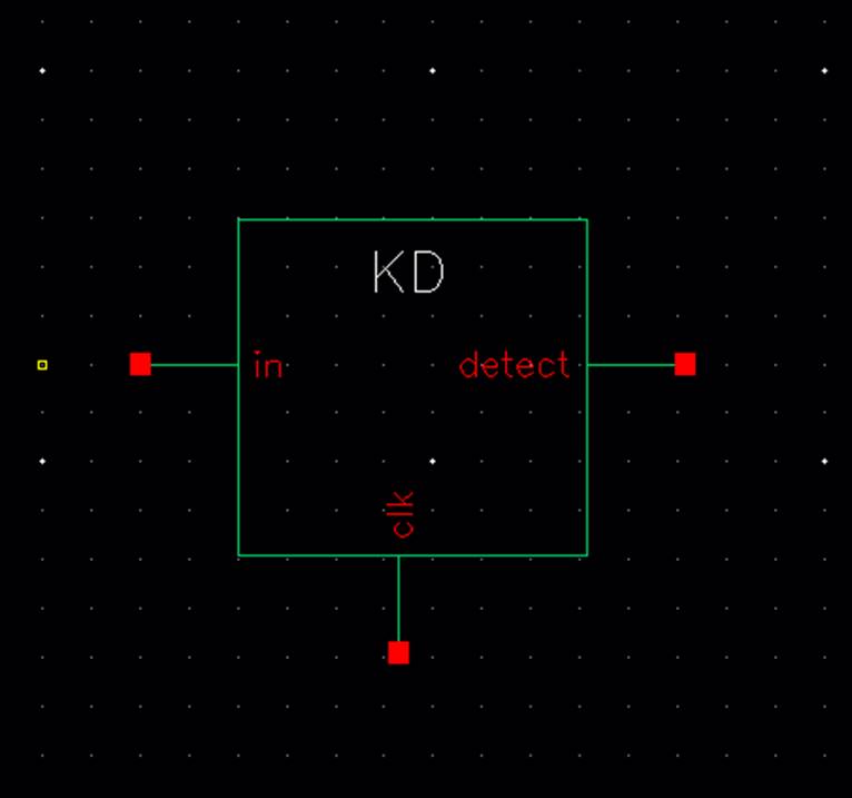
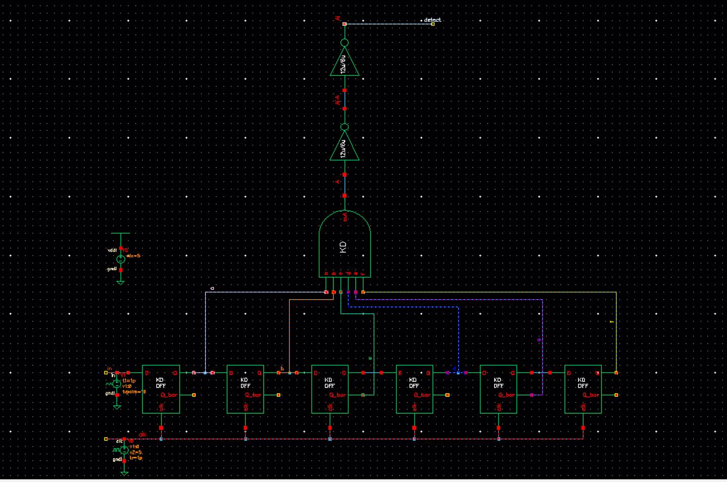
Detector Circuit:
The detector
circuit was easily created using the above components. 6 D flip-flops were tied
together to provide for a serial input. On every clock cycle, the value of the
previous flip flop is passed to the next. In order to detect the sequence
needed, 101011, the correct output from each flip-flop had to be tied to the
AND gate. If a 0 was required on that part of the sequence, then Q bar would be
tied to the AND gate. If a 1 was desired, then Q would be used. When the
selected outputs from each flip-flop matches the sequence desired, the AND gate
outputs a high-level logic, indicating a detection. Below is the full circuit
and symbol created:

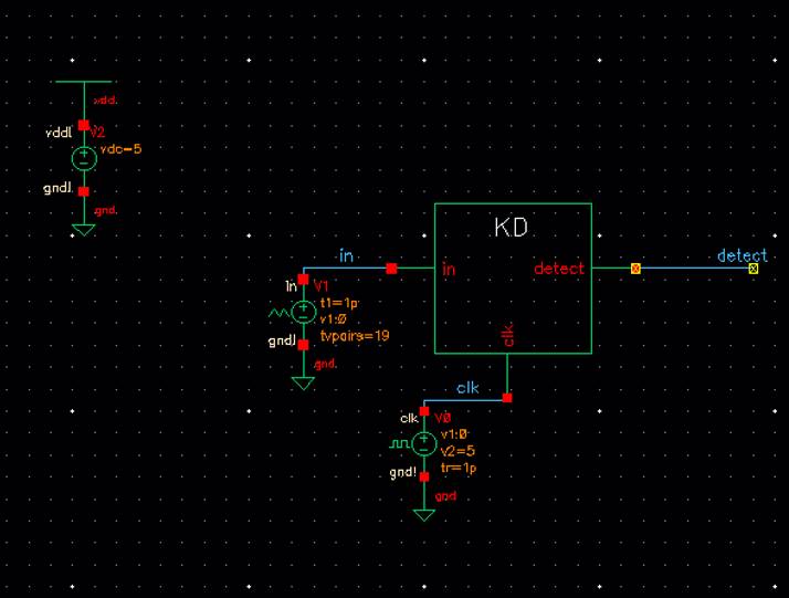
I was able to
successfully simulate the detector circuit using a piece wise linear source on
the input of the circuit. Below is the simulation schematic and results:
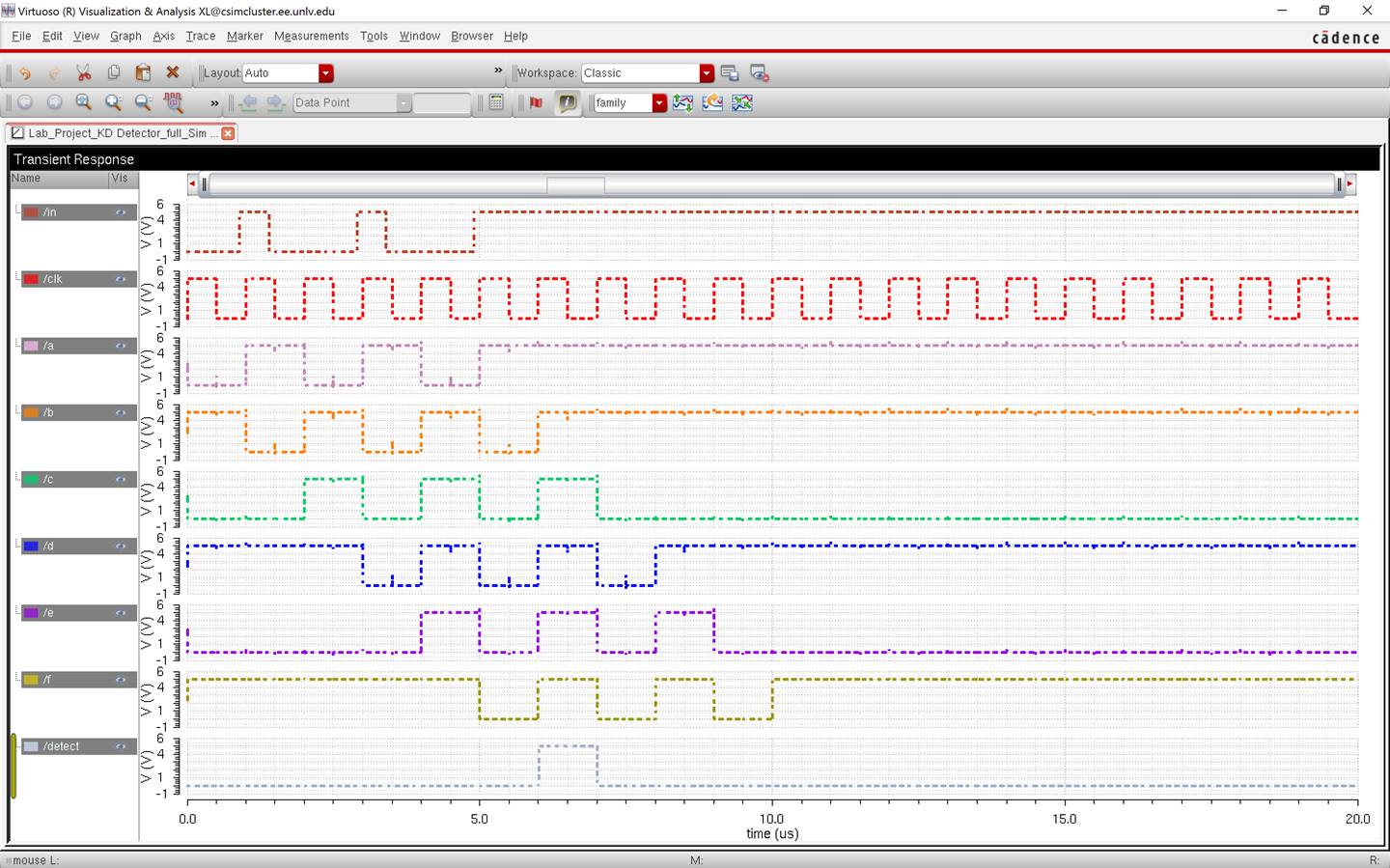
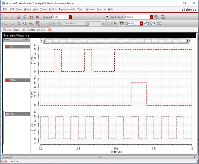
As seen above
the output of the circuit goes when 101011 is fed serially into the input the
output goes high. It returns low after that because the sequence is no longer
there. A buffer was also added to the output which will then be connected to
the bonding pad of the chip.
Below is a
simulation using the symbol of the detector circuit. The same results are seen
as above.
Part 2: Layouts
T-Gate:
Below is the
layout for the transmission gate, which is used in the D flip-flop.
DRC:

LVS:
![]()

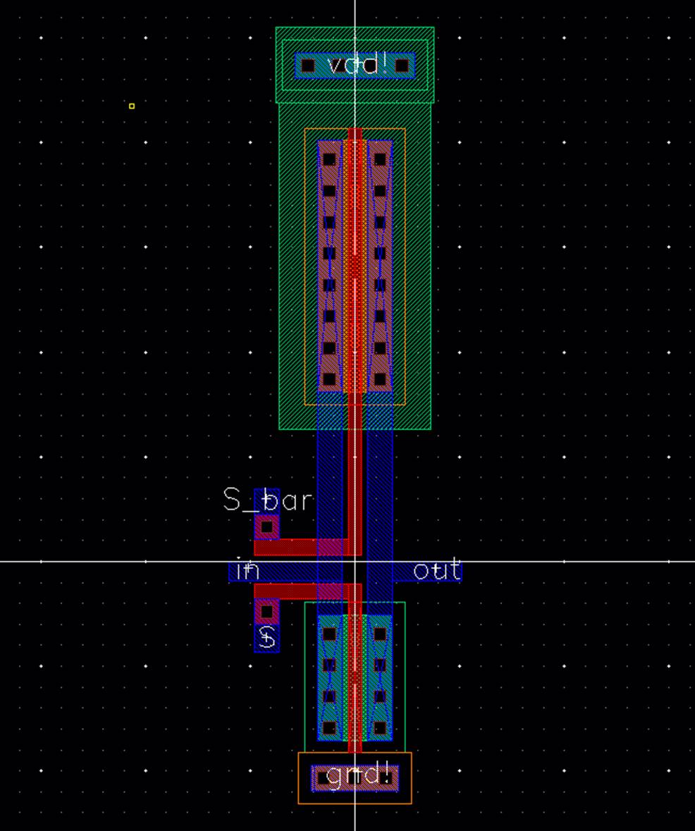
D flip-flop:
Below is the
layout for the D flip-flop, passing LVS and DRC

DRC:
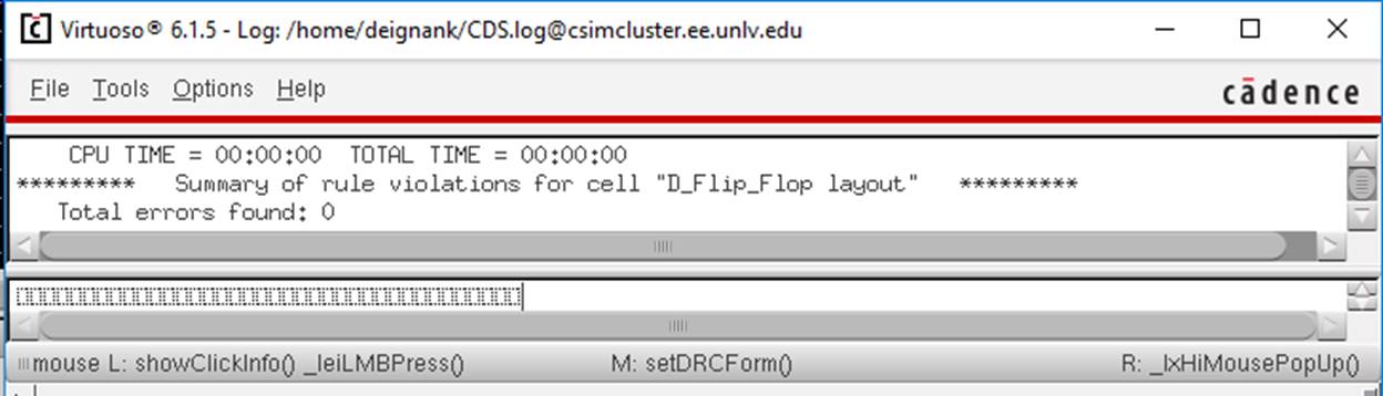
LVS:
![]()
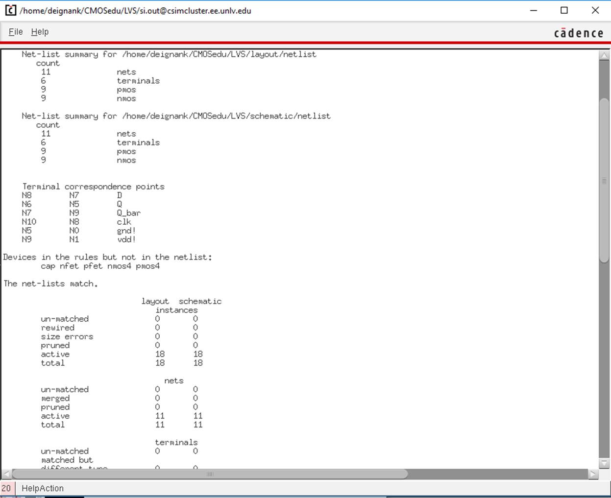
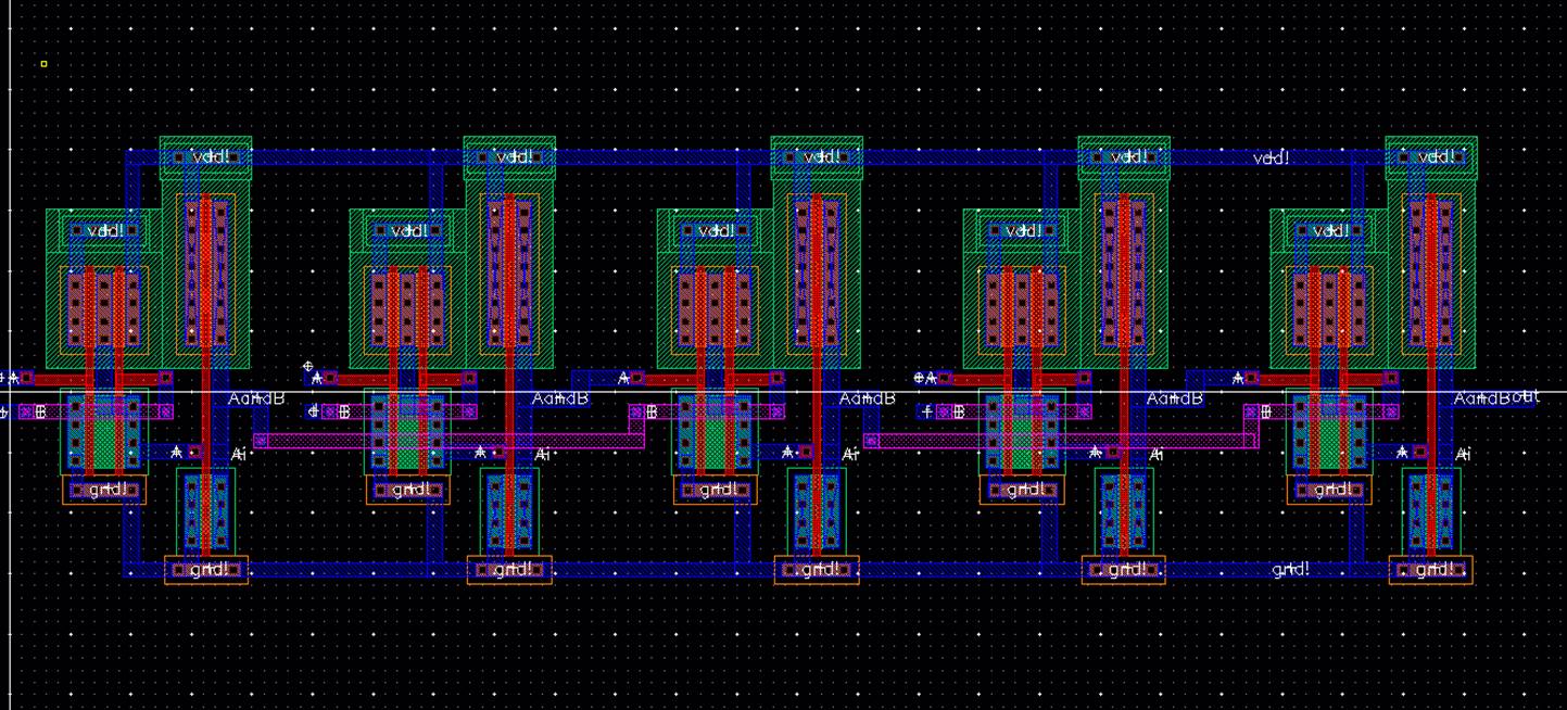
6-Bit AND
Gate:
Below is the
layout for the AND gate, which was made by cascading 5 2-bit and gates.
DRC:

LVS:
![]()

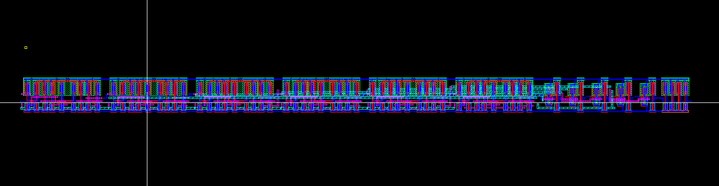
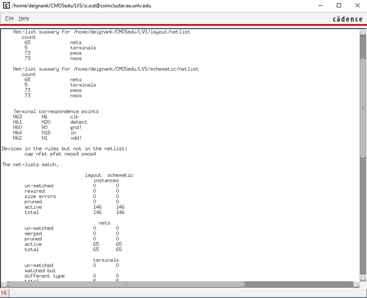
Final Layout
of Detector:
Below is the layout
for the full detector circuit. As shown, it passes DRC and LVS
DRC:

LVS:
![]()
My
design directly can be accessed through this link.