EE421L
"mgill19@unlv.nevada.edu"
Mari Gilligan
Prelab2-pic#1:ADC and DAC
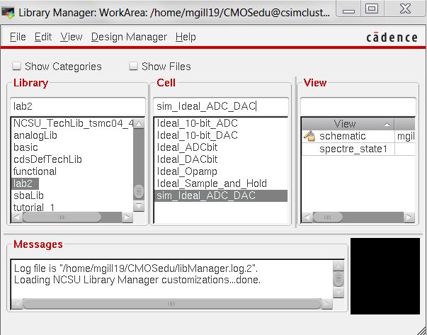
step1:uploading lab 2 which contain this ideal sim for ADC and DAC:
PostLab #2
Modifing
DAC by starting from lib-manager ,right click on Ideal-Sim-ADC-DAC and
Ideal 10-bit DAC.then we go to file -new cell view and creat the
cshematic below :
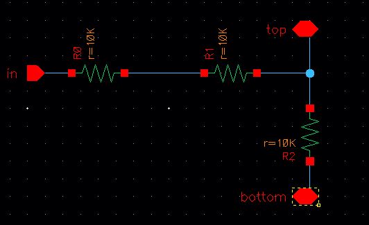
Use 10k ohms resitor and creat the symbol from the schematic above :Creat-cell view -from cell view.
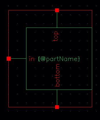
when we have the symbol,its time to go back to new copy of 10bit DAC and replace it with 1-bit DAC ,then we will see :
from this one ,we need to creat symbol like we did earlier.
time
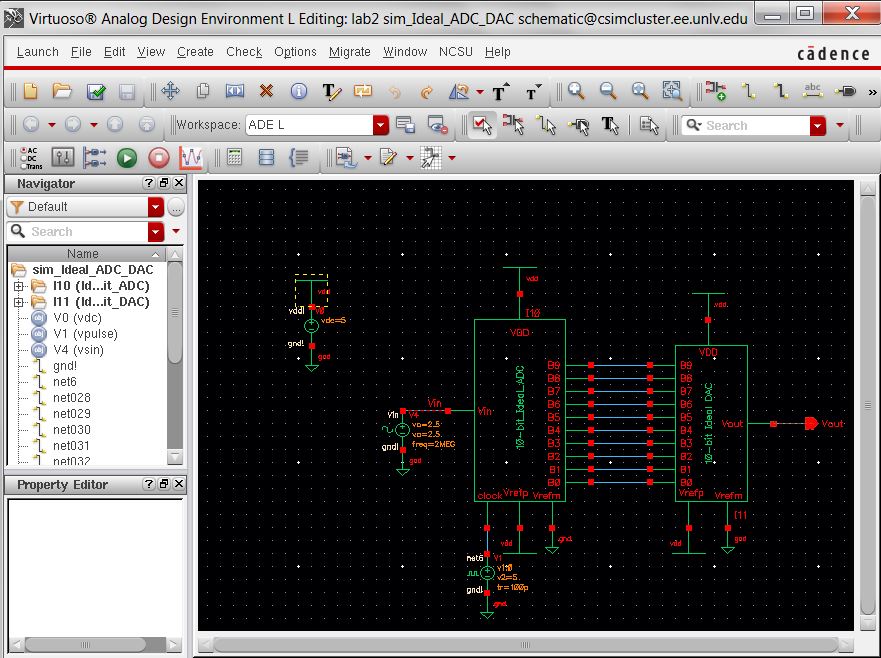
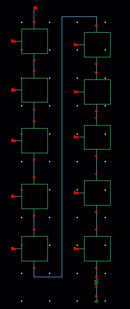
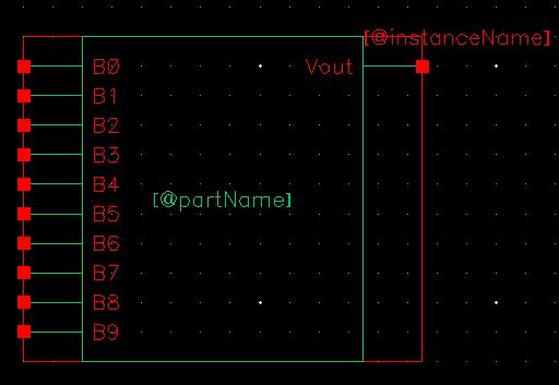
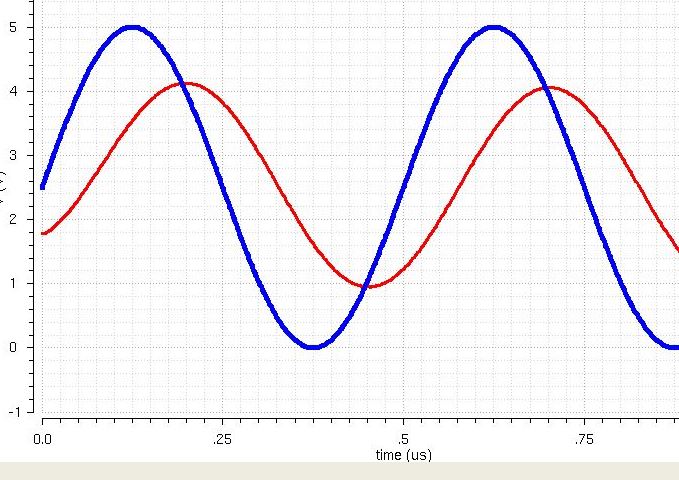
to do the schematic on DAC .go to ADC DAC circuit and replace the ideal
DAC with the new one ,keep in mind you need to take care of the pins.
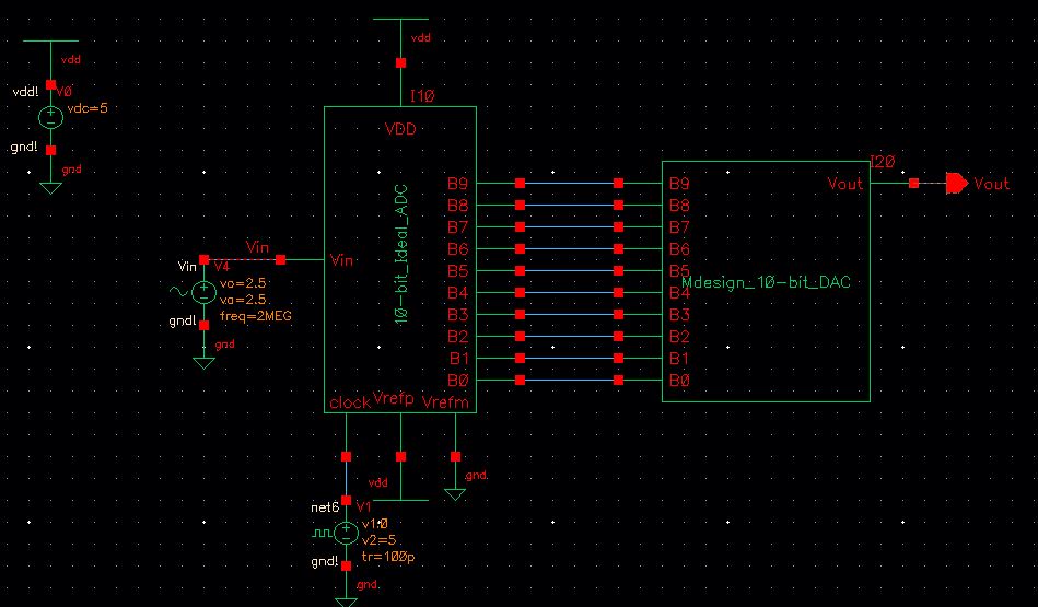
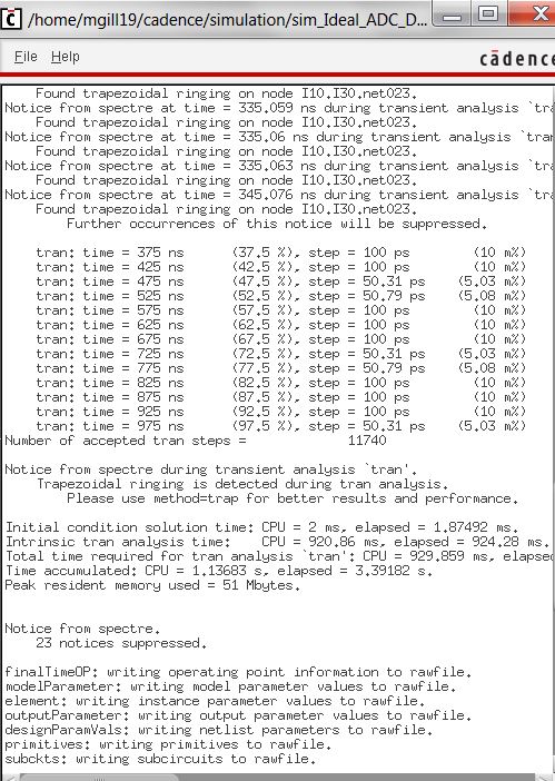
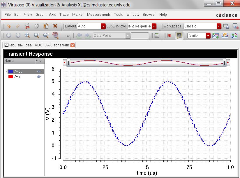
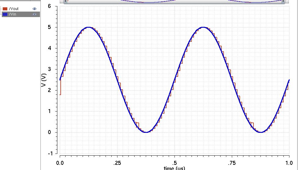
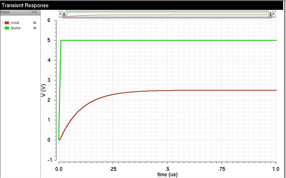
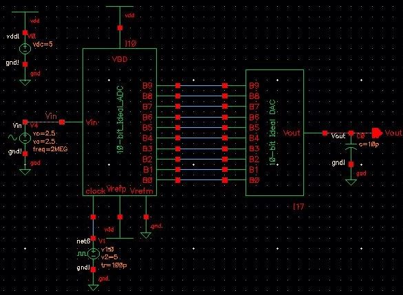
for simulation use the transient with 1u, and we will see an analog to digital conversion like this:
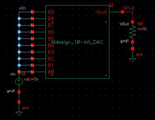
Now i want to determine the output of the resitor ,i can chooce different strategy to do so and i chose to go with sweep:
i will choose the resistor to be RL.
As
you can see i already choose the vin and vout cells that im interested
for my simulation,they have slightly different dashes on the top of
their nodes,then i will go to analysis and do the dc analysis.
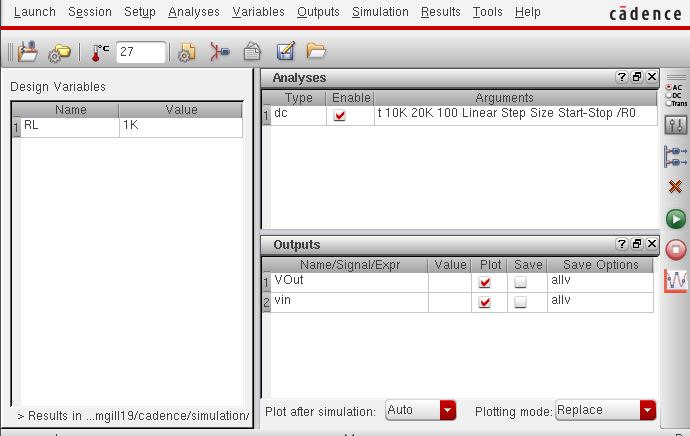
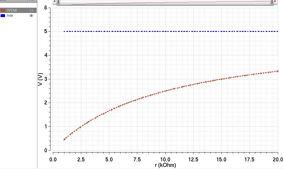
After measuring the r at piont 10.0kohms i will get R=10.01kohms which is close enough to what i suspected to be .
Hand
calculation : i will start with 1-bit DAC and my input pin has 2R and
with be parallel with the other 2R thet i have .after simplifying and
calculating the circuit,i have to reach vin/2 to be 0.7RC .i will set
the Rout and capacitor to 10pf.
cap=10pf.0.7.10k.10p=0.7Microsecend.vin=5v and vout has to be find for
2.5v
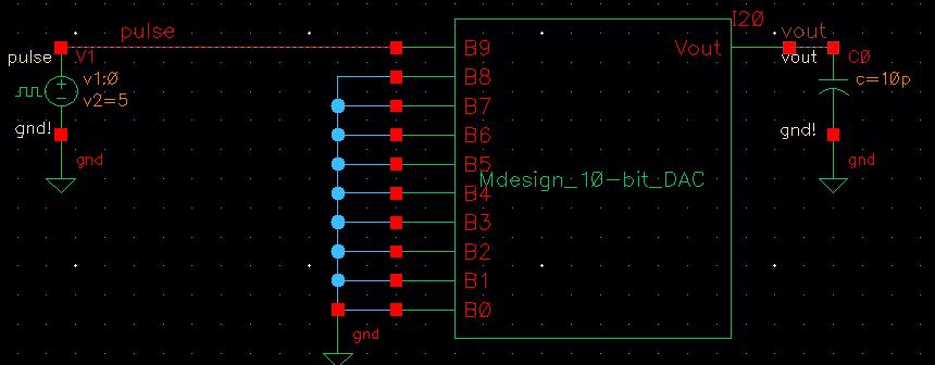
RL and C needs to be attached to the ADC DAC circuit :
we run the simulation to make sure it does work as we expected to be.
R=10k
delay of signal :
the signal increases by capacitor charging and vise versa:
im adding the capacitor to clearly watch the behavour on my simulation,then i explain if i get the right results as i expected.
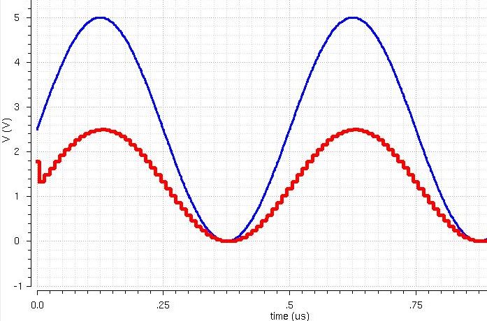
since
we had an Ac signal we saw the amplitude decreses because the capacitor
makes the current to go though it and will effcet the behavour of AC
Signal.
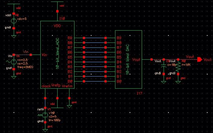
i did combine the R and C,and according to my simulation ,the amplitude decreses because of the leakage current through the C.
If the R has bigger value compare to resistance in the switch then i should have DAC to have more current .
"Return to EE 421L Labs "