Lab 7 - ECE 421L
Authored
by Michael Villalba
1008445138
villalb5@unlv.nevada.edu
10/27/2014
Lab
description
In
this lab we will be creating multiple gates such as OR, NOR, AND, and
NAND gate. We will also create a 8-bit MUX/DEMUX. Then we will also
create a 8-bit full adder which we did in the previous lab.
First thing is to create a 8-bit converter:
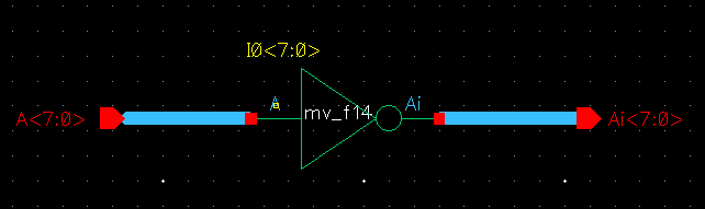
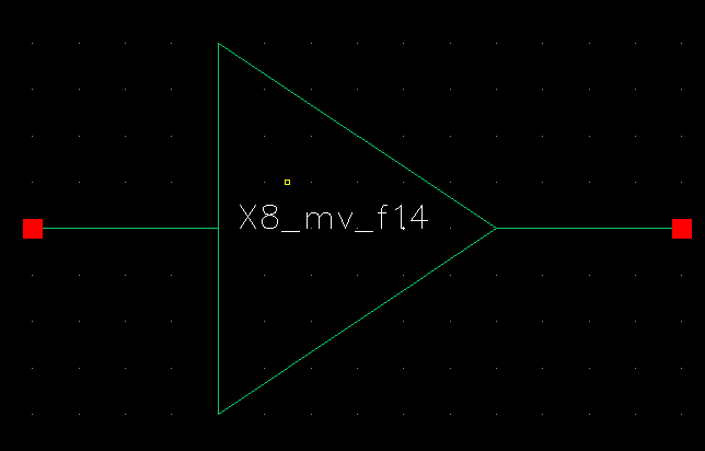
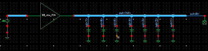
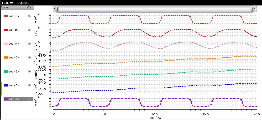
Then I simulated the 8-bit inverter:
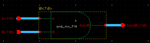
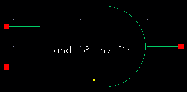
Here is the schematic and symbol for the 8-bit AND gate:
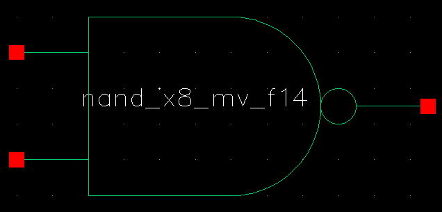
Here is the symbol for the 8-bit NAND gate (which we also did in the previous lab):
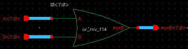
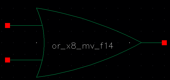
Here is the schematic and symbol for the 8-bit OR gate:
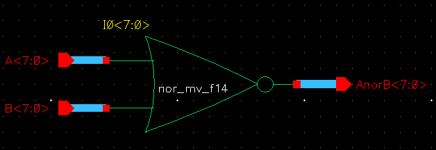
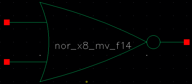
Here is the schematic and symbol for the 8-bit NOR gate:
Now that we have created the AND, NAND, OR, NOR gates we can simulate them.
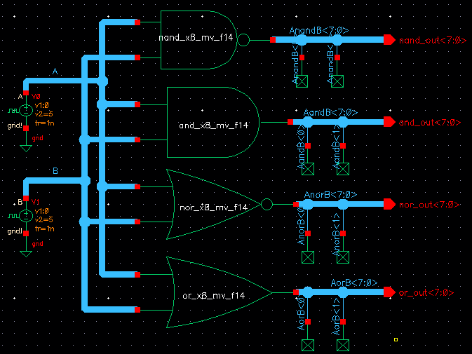
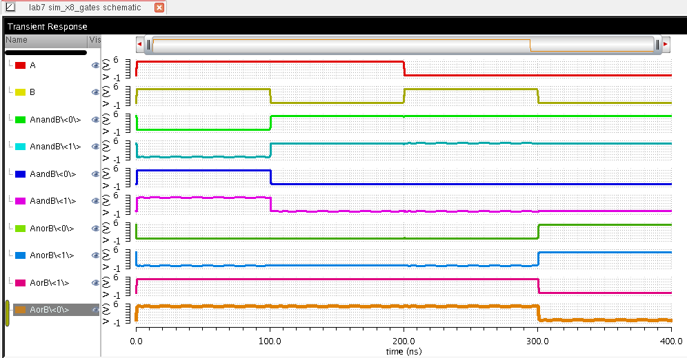
From
the results this show that the OR gate will only be low when both A and
B are low. Then NOR is just the inverted version of a OR gate. The AND
gatewill only give a high output when both A and B are both high. Then NAND is just the inverted version of the AND gate.
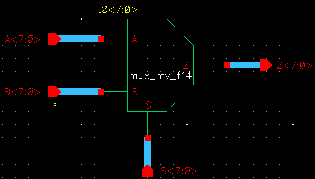
Next
thing we have to do is create a MUX/DEMUX, where a MUX uses the inputs
and turns it into one single output and a DEMUX is the opposite where
it turns one input into multiple outputs.
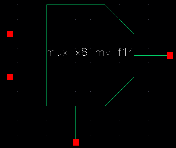
Here is the schematic and symbol for the MUX:
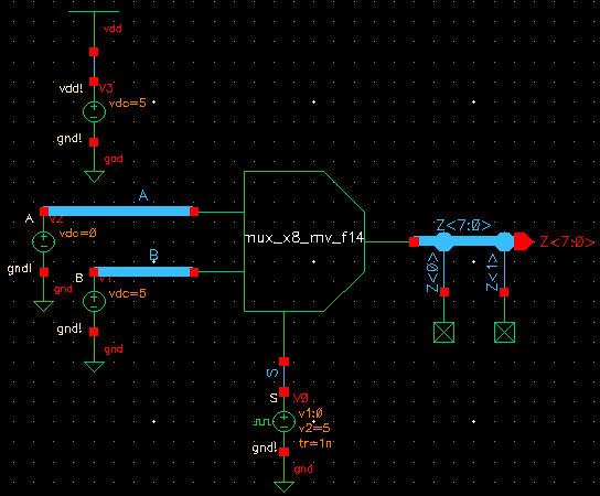
Now we can simulate the MUX to see if what we know about the MUX is correct.
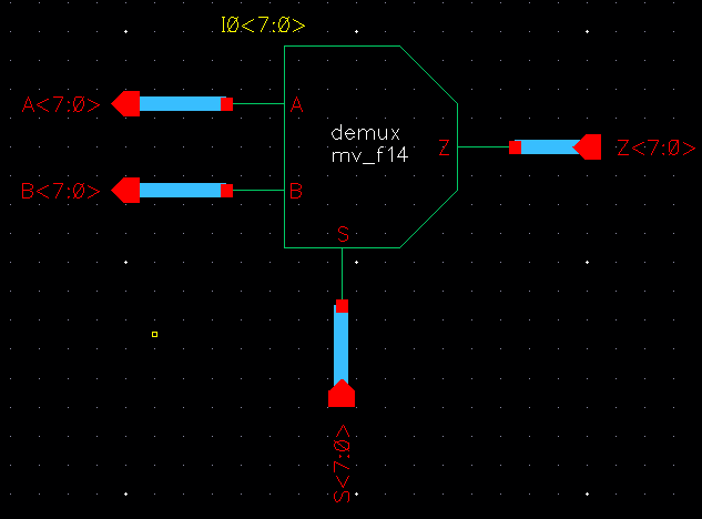
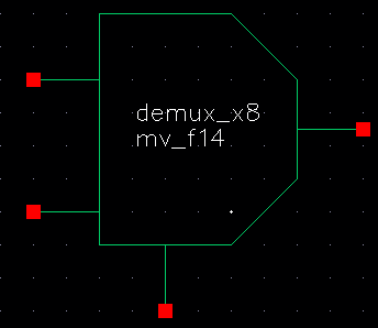
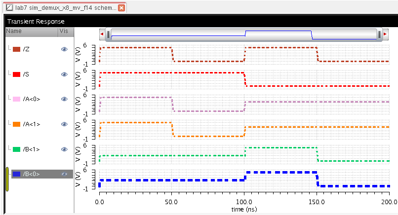
Here is the schematic and layout of the DEMUX:
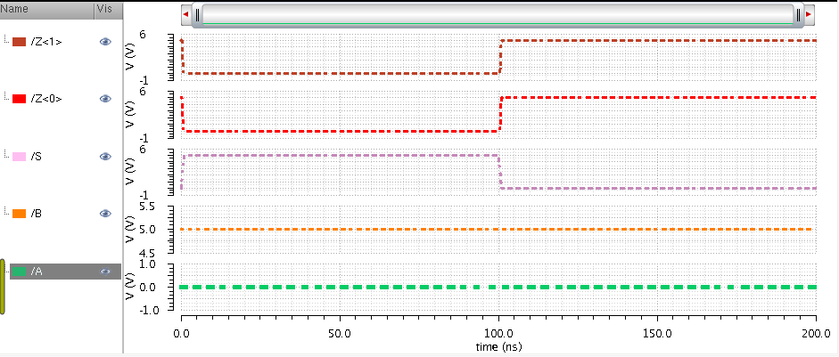
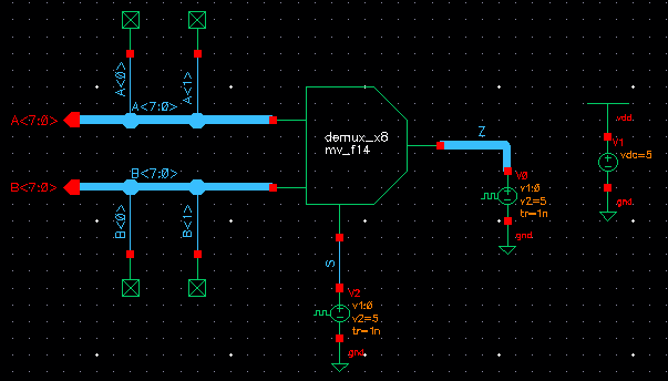
Now that we have created the DEMUX we can now simulate the object.
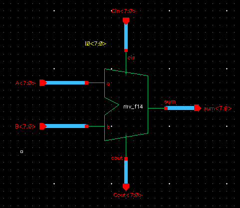
Now we will create an 8-bit Full-Adder. We can use the the full adder from the previous lab to create an 8-bit full adder.
Here is the schematic and the symbol the 8-bit full adder.
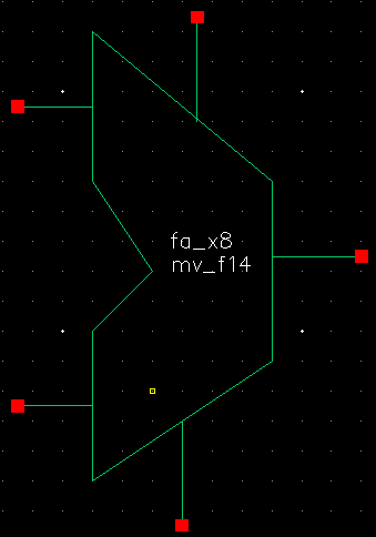
Unfortunately my 8-bit full-adder did not LVS and I was all out of time
to finish the last portion of the lab. I feel like this lab took 3
times longer than all the previous labs
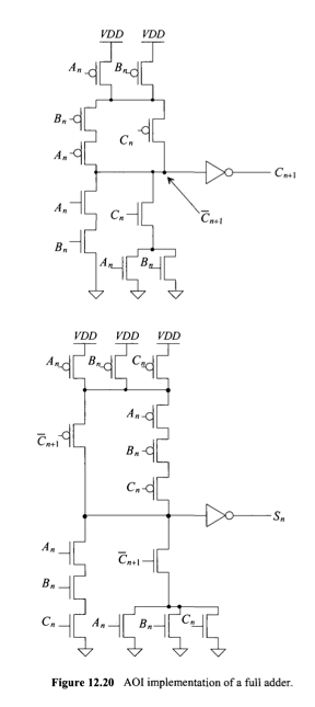
Now we have to create a schematic for figure 12.20
And this concludes lab 7.
Here is proof of me backing up my work

Return to Michael's labs