Lab 6 - ECE 421L
Authored
by Michael Villalba
villalb5@unlv.nevada.edu
1008445138,
10/20/2014
Design, Layout, and Simulatation of a CMOS NAND gate, XOR gate, and Full-Adder.
First
thing we are going to do is use the inverter that was created in Lab 5.
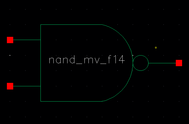
Also from Tutorial_4 we drafted a chematic of a NAND gate.
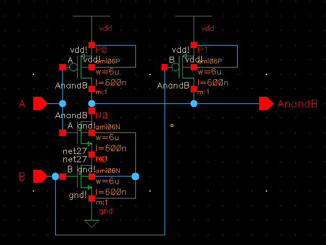
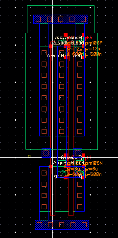
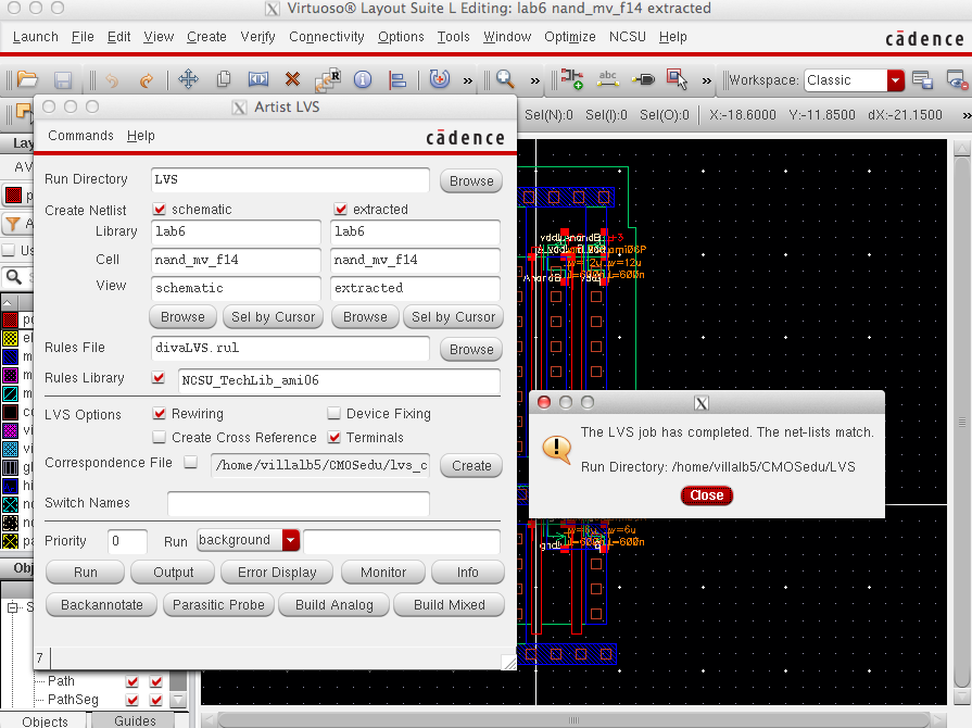
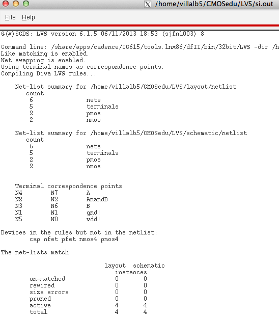
Then we have to ceate a Layout for the NAND gate
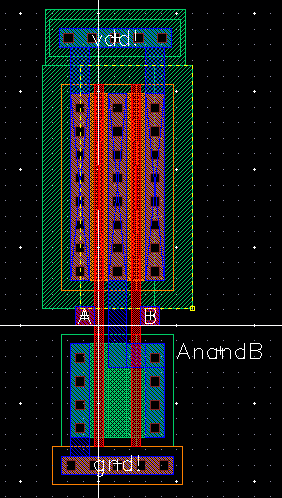
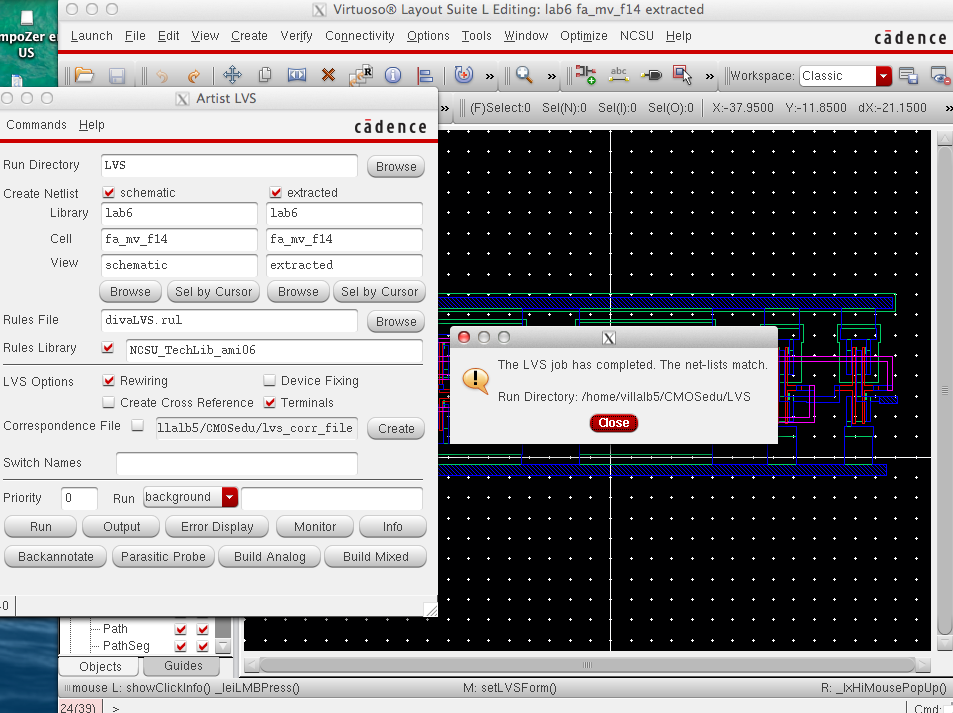
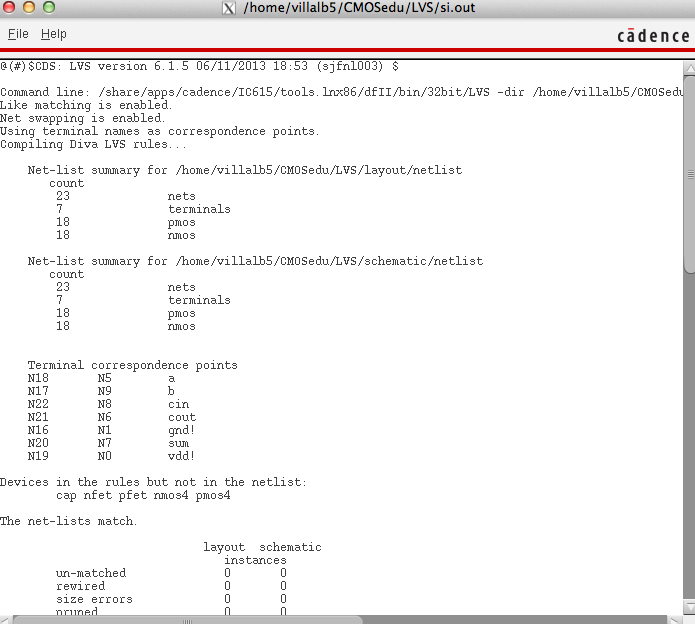
Then we have to extract the layout and perform an LVS to make sure they match
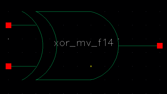
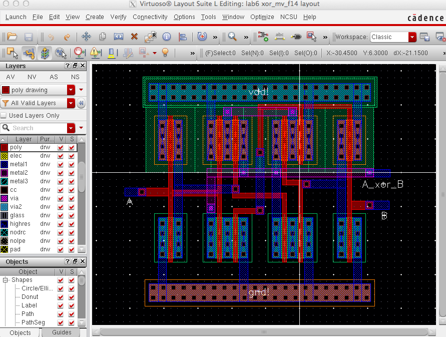
Then we have to create a schematic, symbol and layout for a XOR gate with 6u/0.6u MOSFET
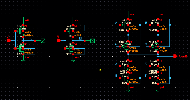
Same
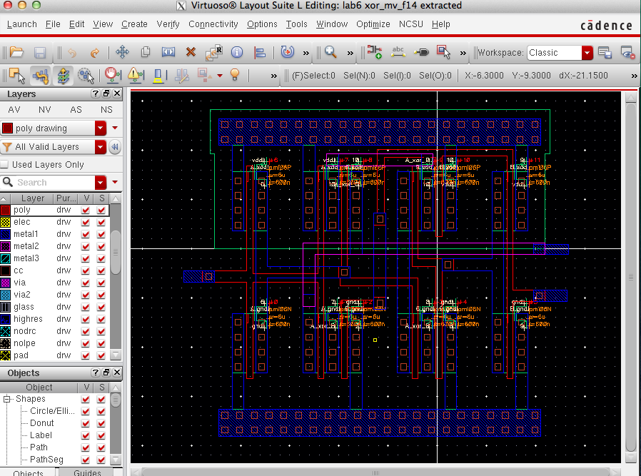
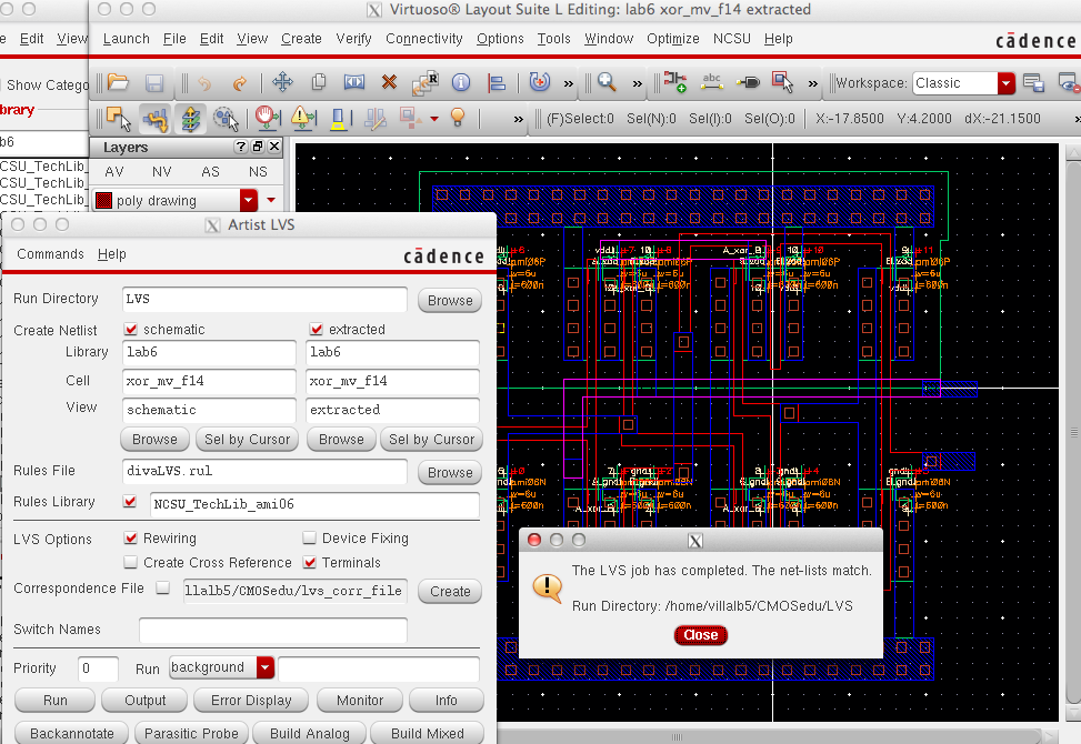
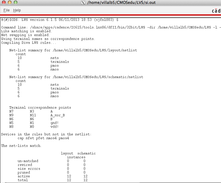
as the NAND gate we need to create a layout and extract the layer then
LVS to make sure it matches the schematic. This layout is more complex
than the NAND gate we created previously.
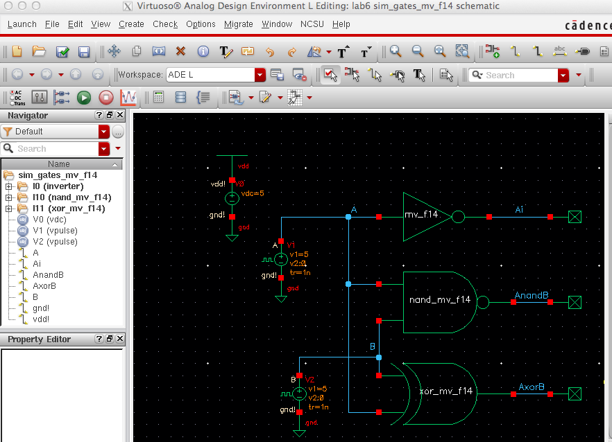
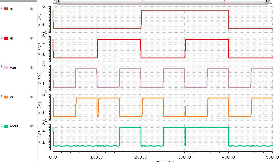
We
are now going to simulate all the gates we created to make sure they
work. the schematic used to simulate them can be seen below. We use
pulse A and pulse, B whos frequency is twice as fast as A to simulate
inputs 00,01,10,11
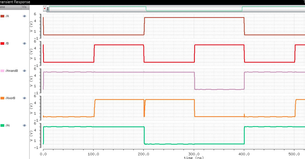
It
is important to realize there is a rise time and a fall time in this
switching between signals. If we look at around the 200 ns mark we can
see a glitch, that is because the numbers are in transition from 01 to
10 but what in between that time the computer is only reading 00,
so 0 or 0 is zero as seen in this glitch.
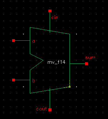
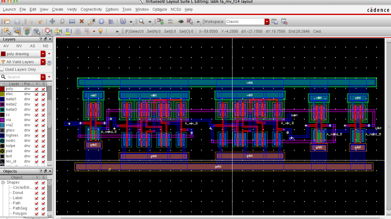
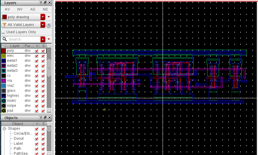
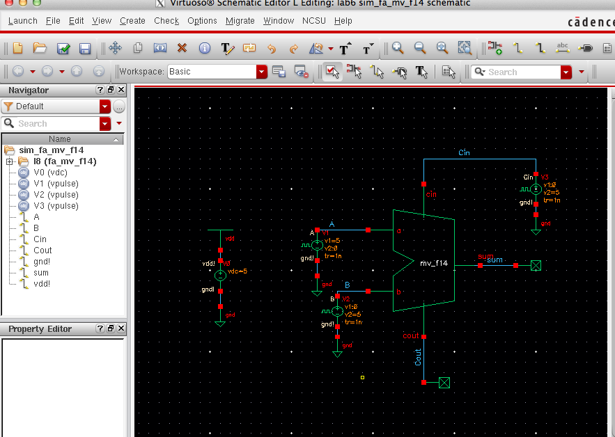
First thing to do is to create a schematic of the full-adder and then the symbol.
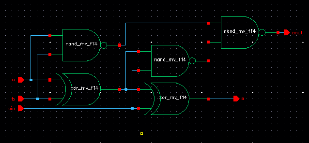
After
creating the schematic and symbol for the full-adder we then have to
create a layout, extract the layout and then LVS the schematic and
extract to make sure they match.
Last thing we have to do is simulate the full adder to make sure its complete.
Here is proof of me backing up my work
lab6 can be downloaded here
Return to Michael's Labs