EE 421L Digital Integrated Circuit Design - Lab 8
Authored by:
Elizabeth Baldivias, Michael Villalba, Taylor Rasmusson, Nick Repetti
baldivi3@unlv.nevada.edu, villalb5@unlv.nevada.edu, rasmuss@unlv.nevada.edu, repettin@unlv.nevada.edu
December 1st, 2014
Generating a test chip layout for submission to MOSIS for fabrication.
LAB WORK
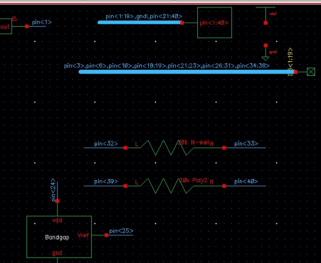
We based our layout on the following schematic.
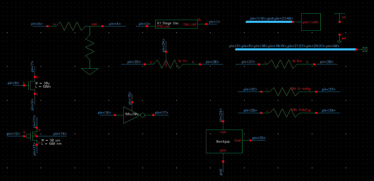
Our chip included the following test structures.
Layout: 30u/0.6u NMOS

30u/6n PMOS

Inverter made using 30u/0.6u NMOS and 60u/0.6u PMOS

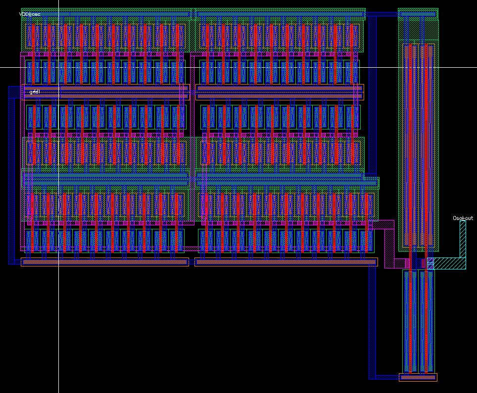
Following is an image of the 61 ring oscillator.
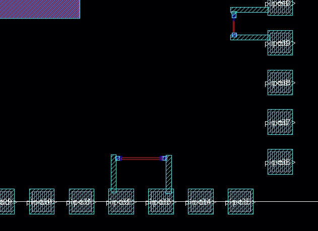
We also made a 20k nwell resistor.

20k hi-res poly resistor

1k n+ resistor.
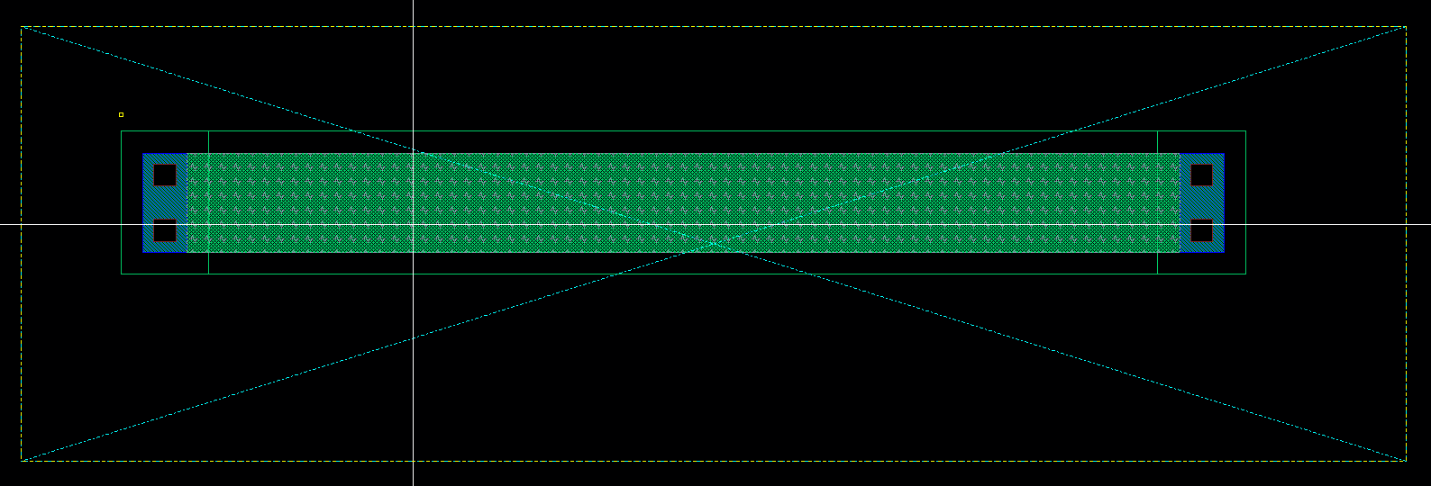
1k p+ resistor
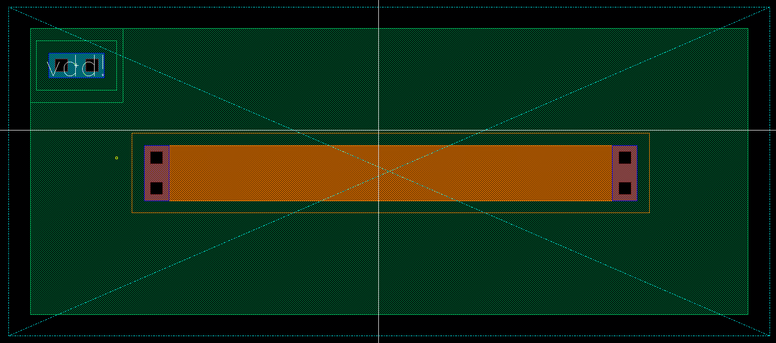
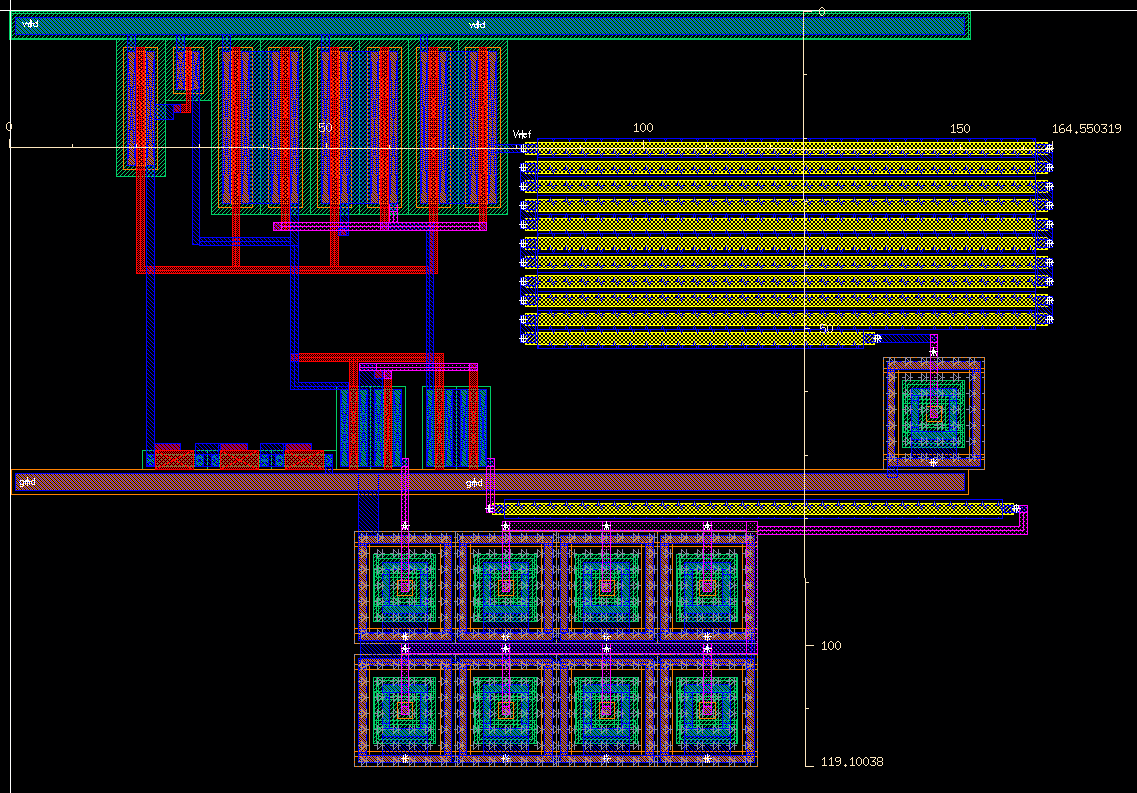
Here is the design used from EE421 project for Bandgap reference
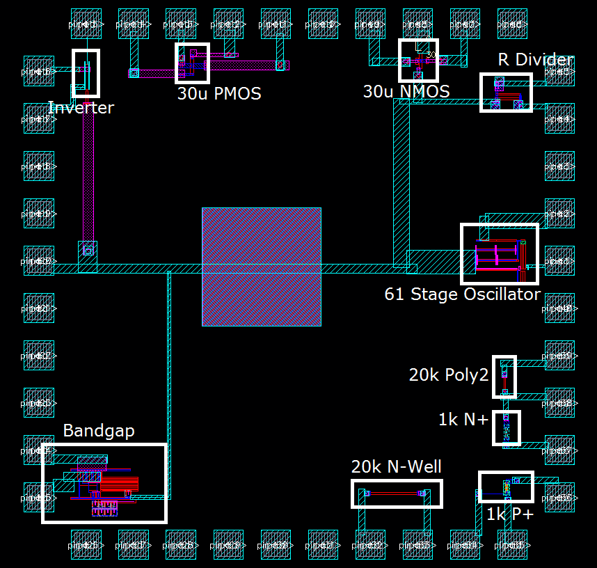
Here is the result of all our parts put together.
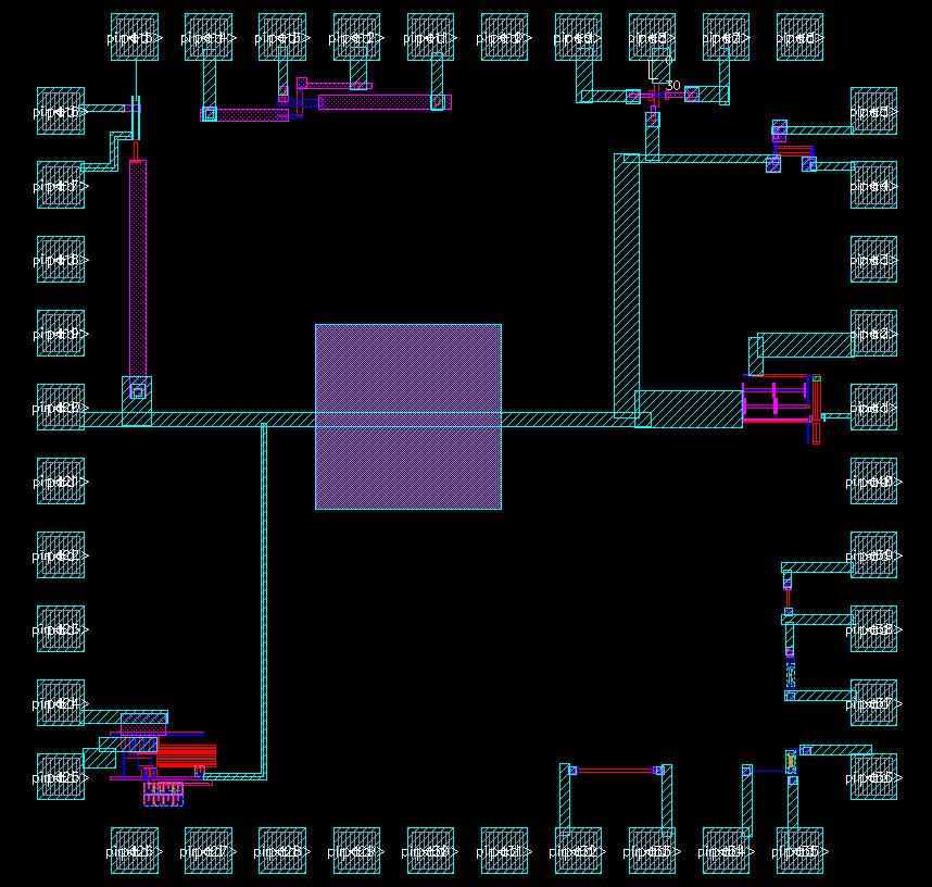
Here is the chip layout with labels.

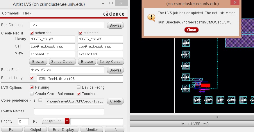
Our
layout did not LVS because it was not working with n+ and p+ resistors
due to the nodrc layer we had on. To test that the other parts of the
chip would LVS, we took out the resisors and the LVS worked. Here is
the schematic that we used without the resisitors and the verification
that the LVS worked.


How to Test the Chip
Note that all of the devices have their own power so that one of the devices doesnt break the whole chip.
Connect gnd to pin20
NMOS
- To conect to NMOS: pin7 drain, pin8 gate, pin9 source
PMOS
- To connect to PMOS: pin11 source, pin12 gate, pin13 drain, pin14 body
Inverter
- To connect to inverter: pin15 is vdd of inverter, pin16 input of inverter, pin17 output of inverter
Ring oscillator
- Can be used to test the speed of a particular part in the circuit
- To connect to ring oscillator: pin1 osc_out, pin2 vdd of oscillator
20k N-Well resistor
- To connect to N-Well resistor: pin32 left terminal, pin33 right terminal
20k High-Res poly resistor:
- To connect to 20k High Res poly resistor: pin39 left terminal, pin40 right terminal
1k nplus resistor
- To connect to 1k nplus resistor: pin37 left terminal, pin38 right terminal
1k pplus resistor
- To connecto 1k pplus resistor: pin34 vdd, pin35 left terminal, pin36 right terminal
Bandgap
- Maintains a stable voltage at 1,25V even if there is a shift in VDD
- To connect to bandgap: pin24 vdd of bandgap, pin25 vref (vout of bandgap)
Click here to download all the contents of the chip.
The entire schematic and layout can be found in the cell called top9.
Note that the LVS will only work without the n+ and p+ resistors. (see cell top9_without_res)
Return to EE421 labs here.
