Lab 5 - ECE 421L
After
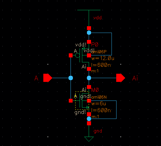
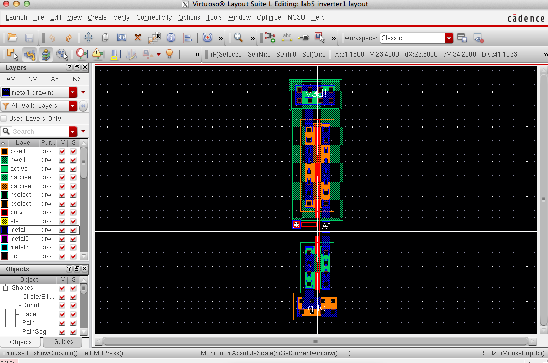
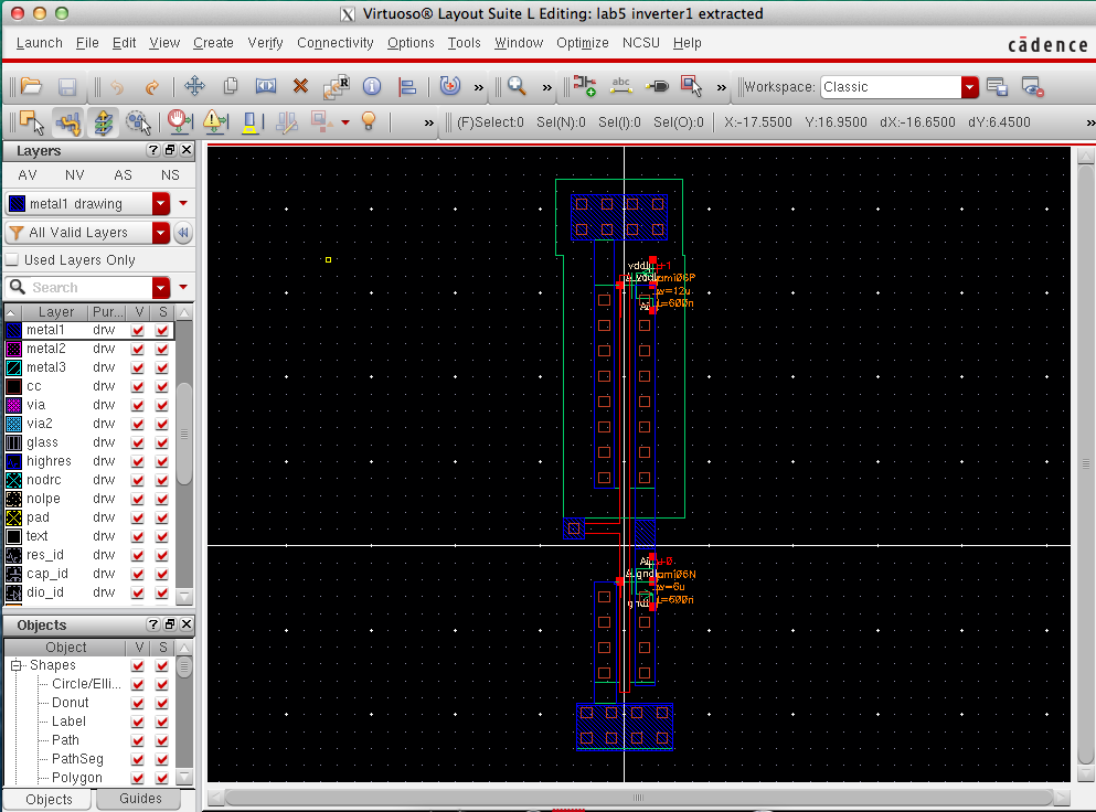
creating the layout we need to DRC to make sure it passes and that
there are no errors. Once it passes we can now extract the layout.
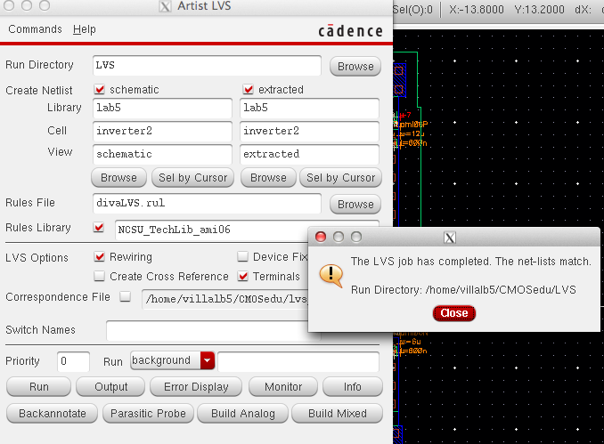
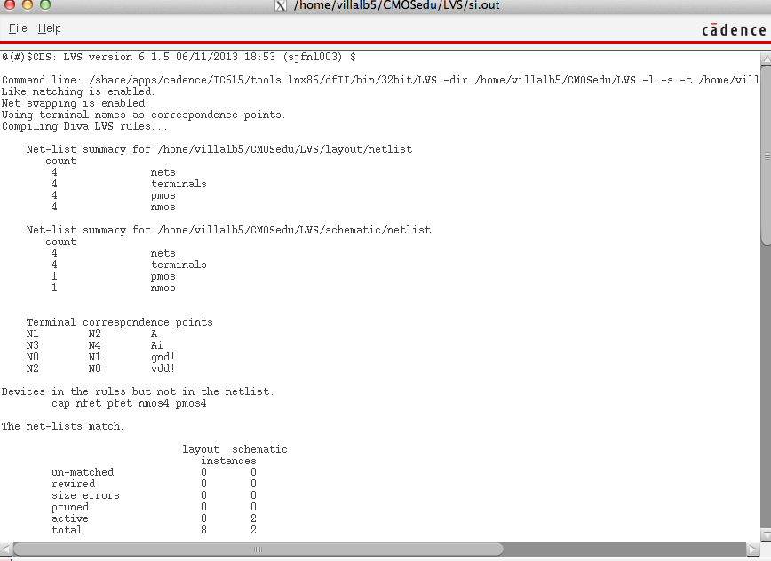
Now that we have our extraction LVS our schematic with the extraction to make sure they match.
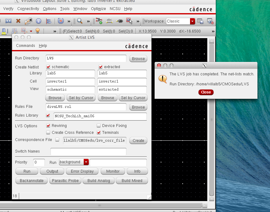
We
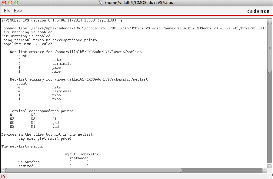
get the notification that the LVS is a match but we still want to check
the output of the LVS just for a double confirmation.
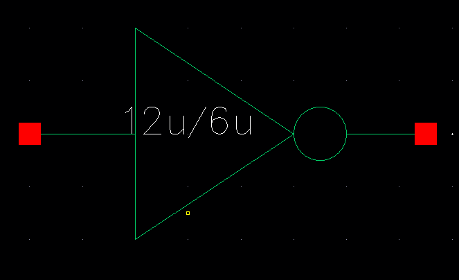
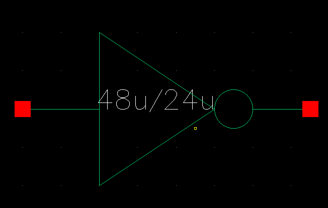
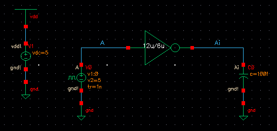
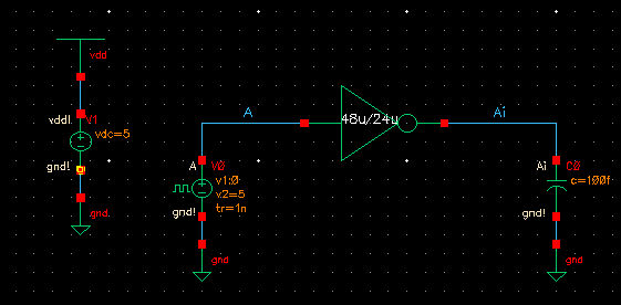
48u/24u symbol:
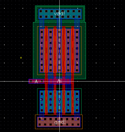
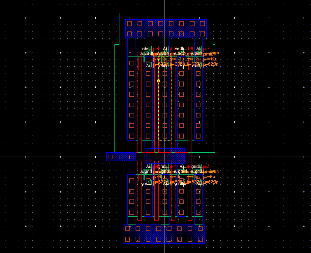
Extraction:
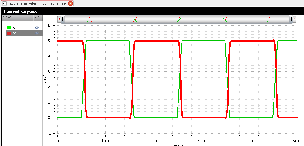
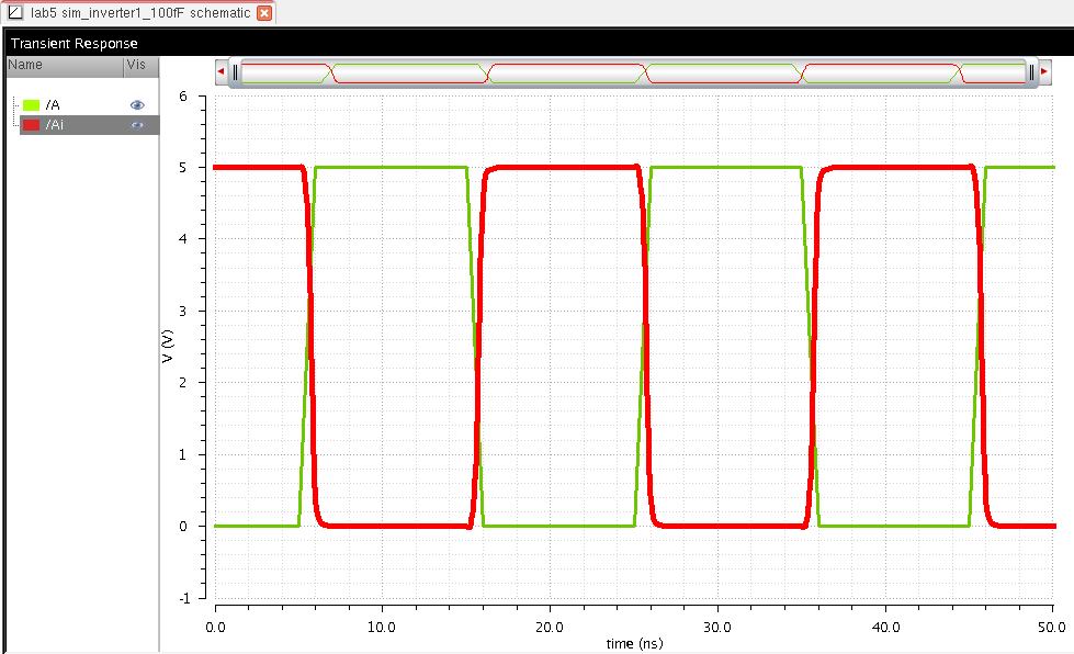
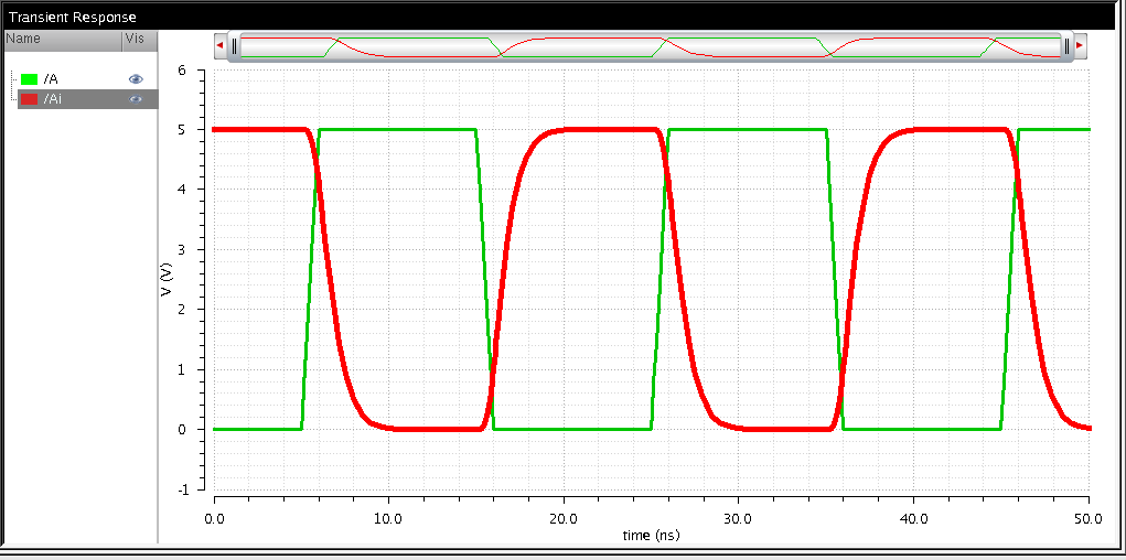
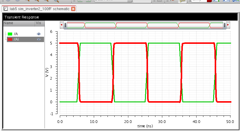
100fF:
Spectre UltraSim
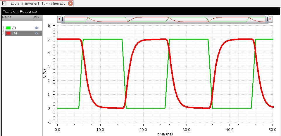
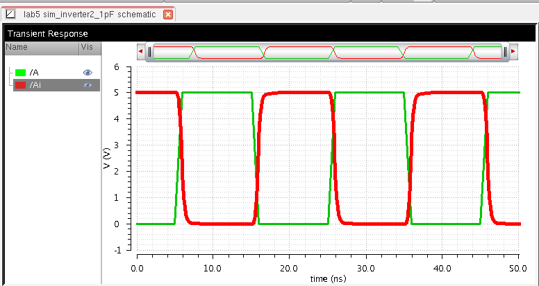
1pF:
Spectre UltraSim
Spectre UltraSim
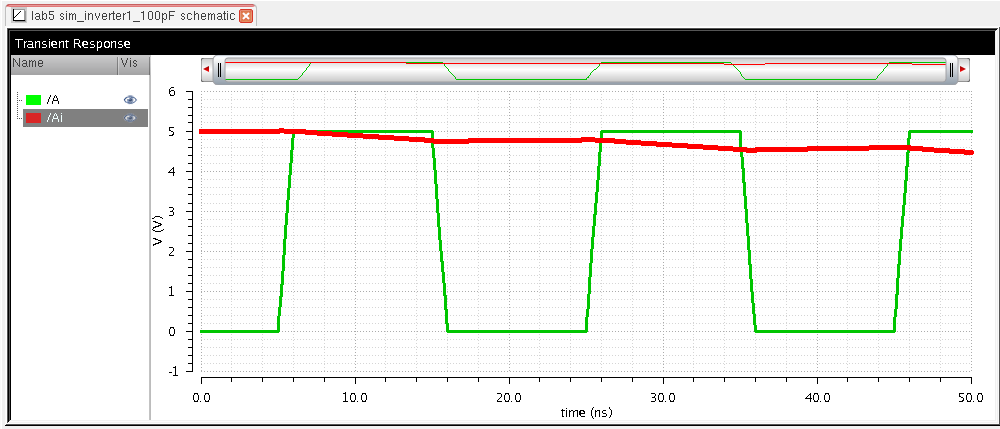
100pF:
Spectre UltraSim
Now we will run the same simulations for the 48u/24u inverter.
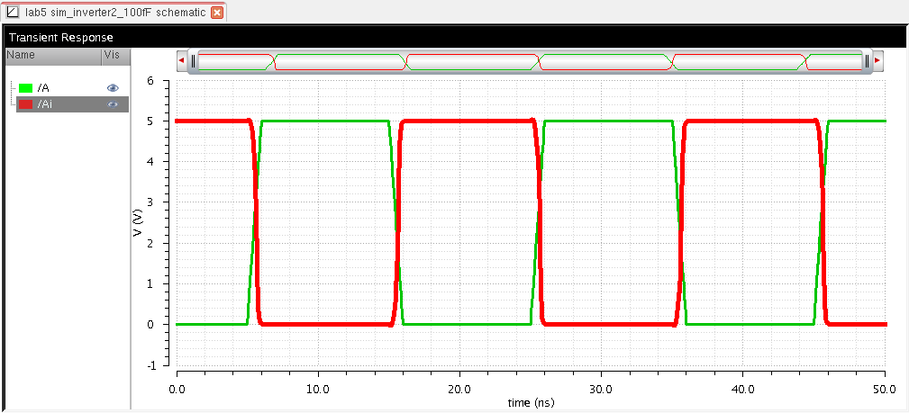
100fF:
Spectre UltraSim
1pF:
Spectre UltraSim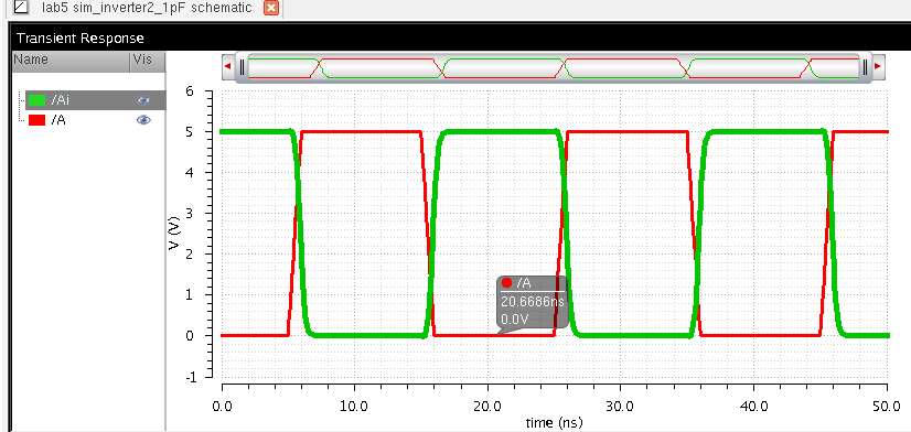
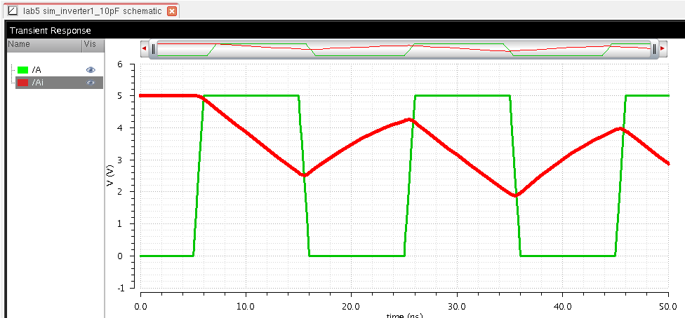
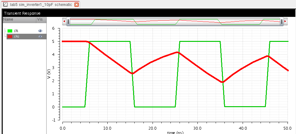
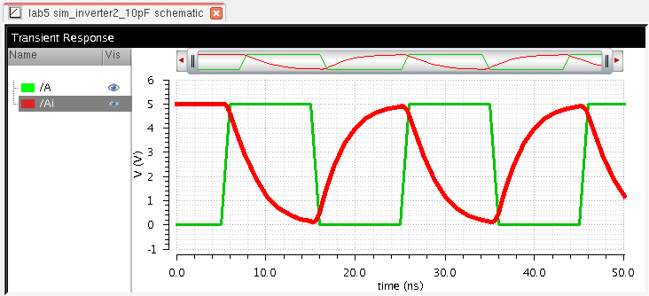
10pF:
Spectre UltraSim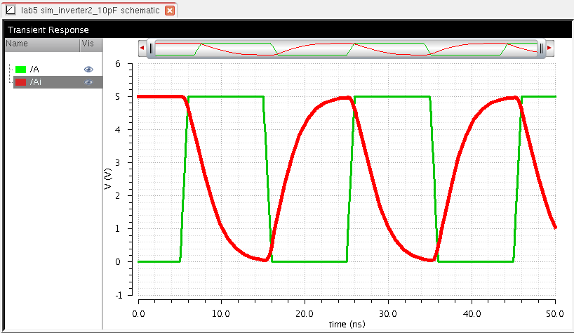
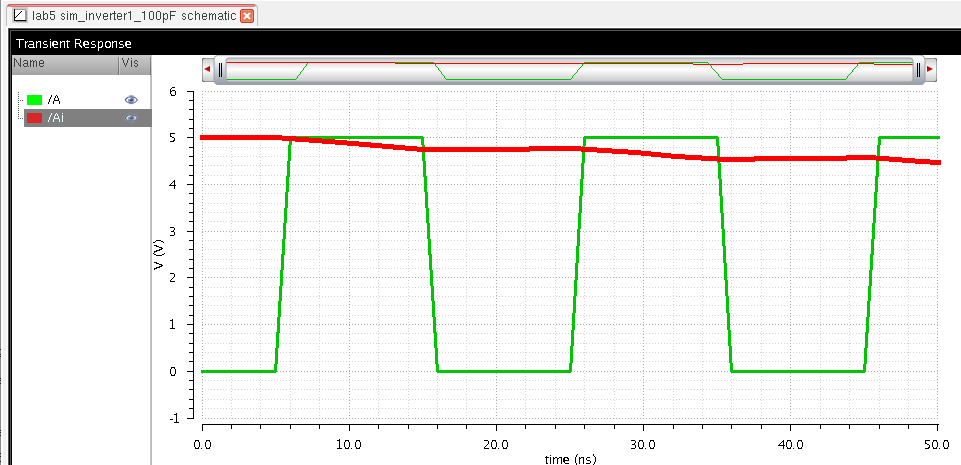
100pF:
Spectre UltraSim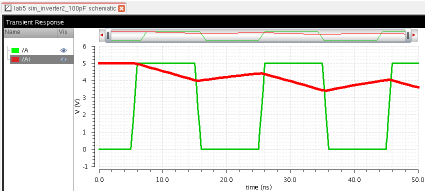
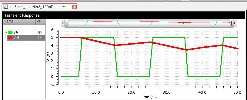
From
the simulations we see that the smaller the capacitance load, the
faster the charge and discharge. The difference between the 12u/6u
inverter and the 48u/24u inverter is that the 48u/24u inverter seems to
charge and discharge faster due to the increased width that allows more
current passing. There wasn't too much of a difference with the
UltraSim, just wasn't as accurate but still good enough to use for
future simulations.
This concludes lab 5!
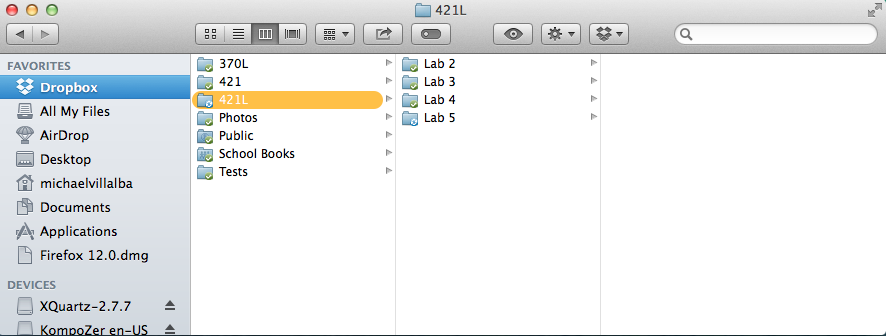
Here is me backing up my work to dropbox.