Lab 4 - ECE 421L
Authored
by Michael Villalba 1008445138,
10-6-2014
The purpose of this lab is to create a layout of NMOS and PMOS devices in ON's C5 process.
First
thing to do is create a new library in Cadence for Lab 4. Then copy all
the cells needed from tutorial_2 into lab 4 and also create cells for
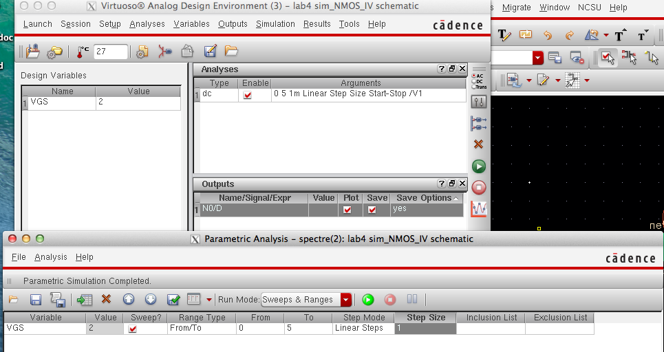
NMOS and PMOS. The graphs that we will generate is ID vs VDS. To perfom
dc sweep for the schematics it must be done in parametric analysis within the ADE L window.
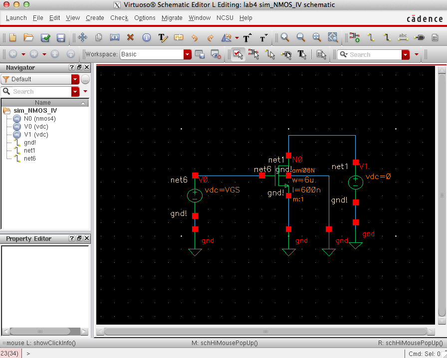
Schematic for NMOS simulation with the W/L ratio being 6u/600n.
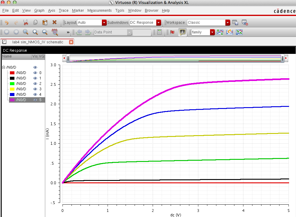
ID
vs VDS for VGS varying from 0 to 5 V in 1 V steps while VDS varies from
0 to 5 V in 1 mV steps. Then running the simulation in parametric
analysis tab to generate the required curves.
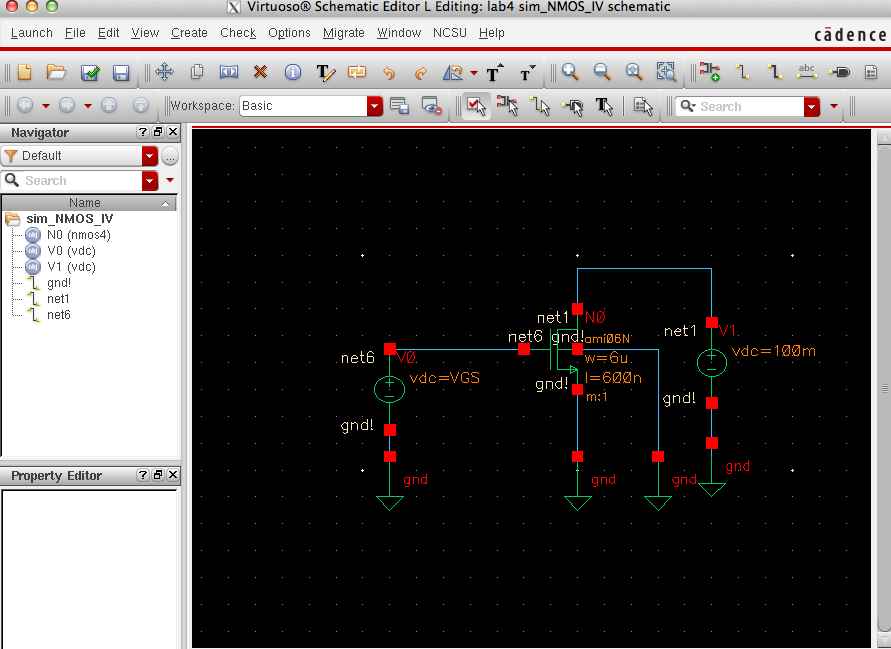
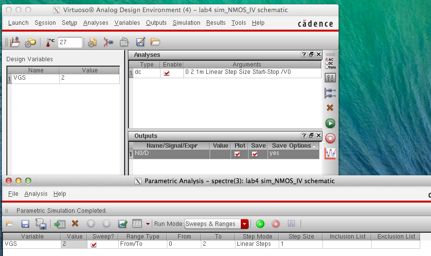
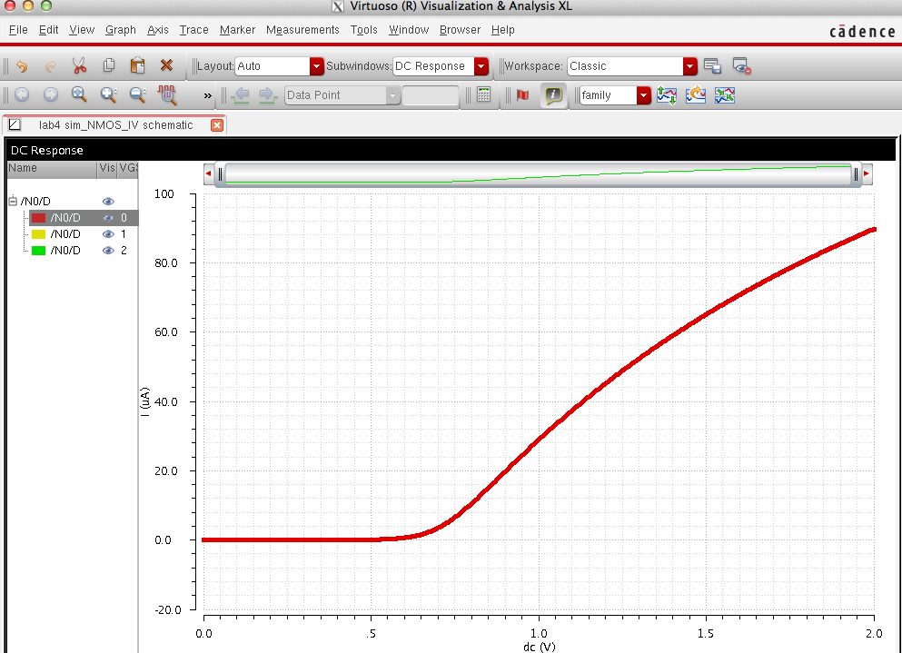
Now we have to create a ID vs VGS (VSG) graph sweeping VGS ans VSG from 0 to 2V in 1mV steps where VDS=100mV
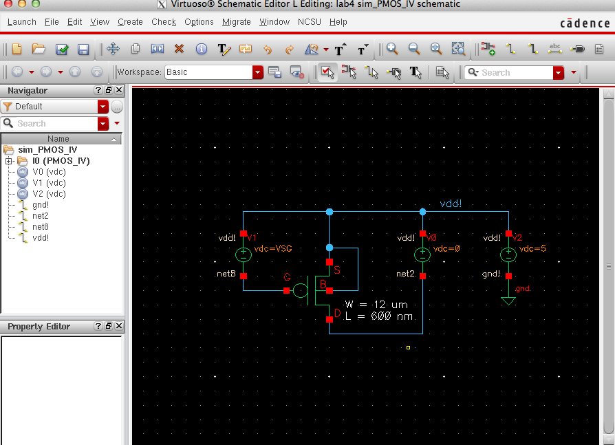
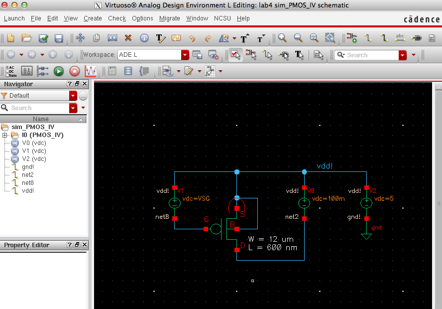
 Now we will perform the same steps for the PMOS schematic.
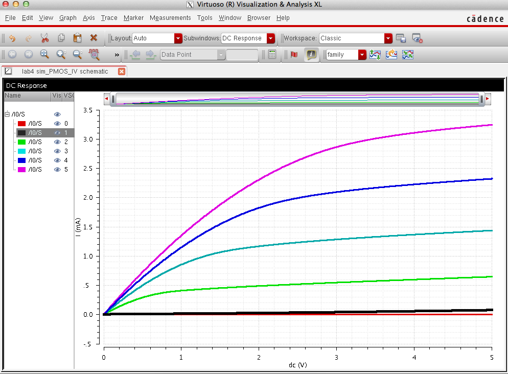
ID vs VDS for VSG varying from 0 to 5 V in 1 V steps while VDS varies
from 0 to 5 V in 1 mV steps. Then running the simulation in parametric
analysis tab to generate the required curves.
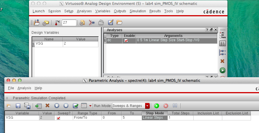
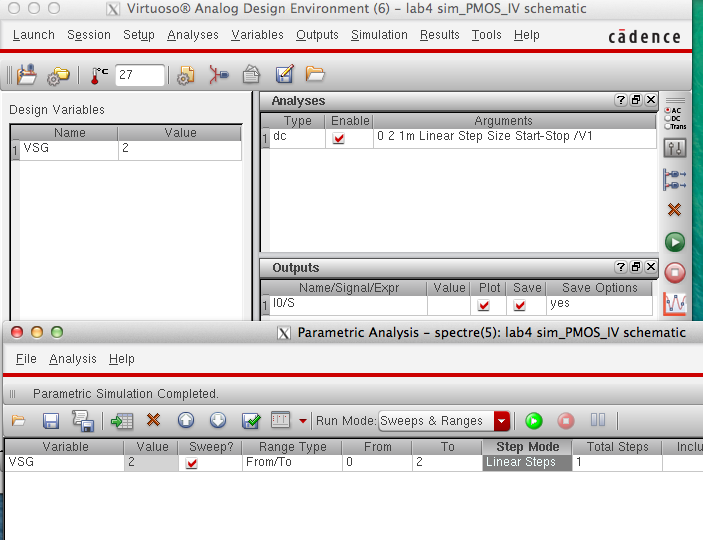
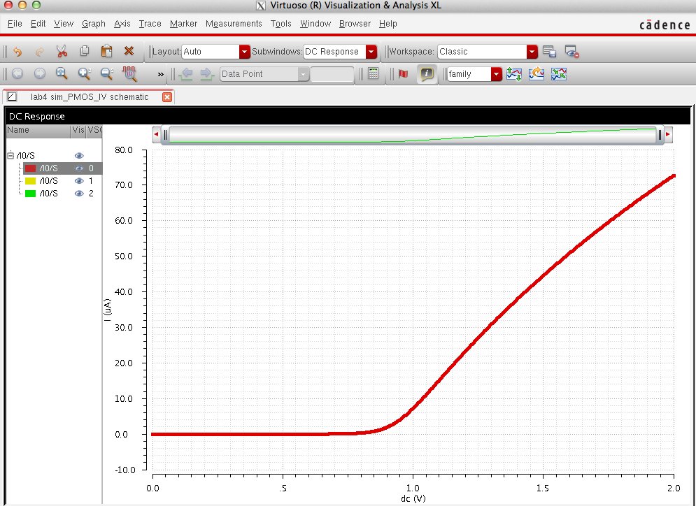
ID v. VSG of a PMOS device for VSD = 100 mV where VSG varies from 0 to 2 V in 1 mV steps.
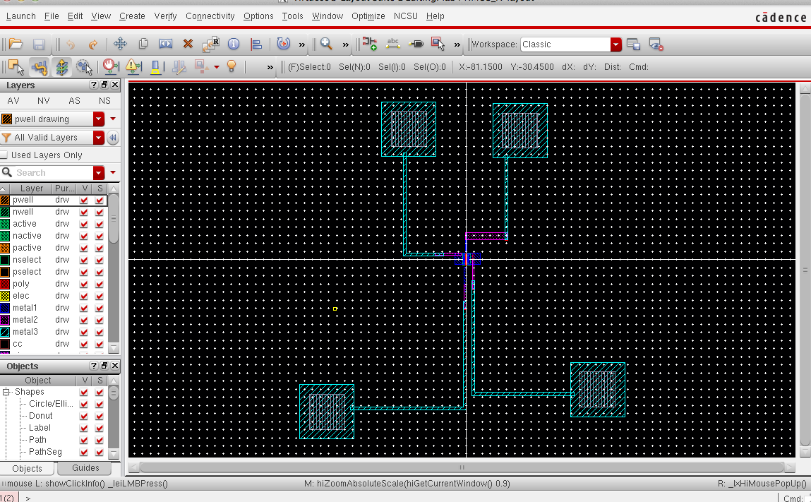
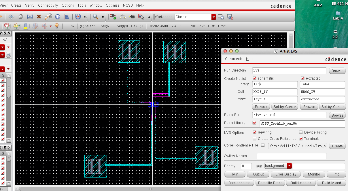
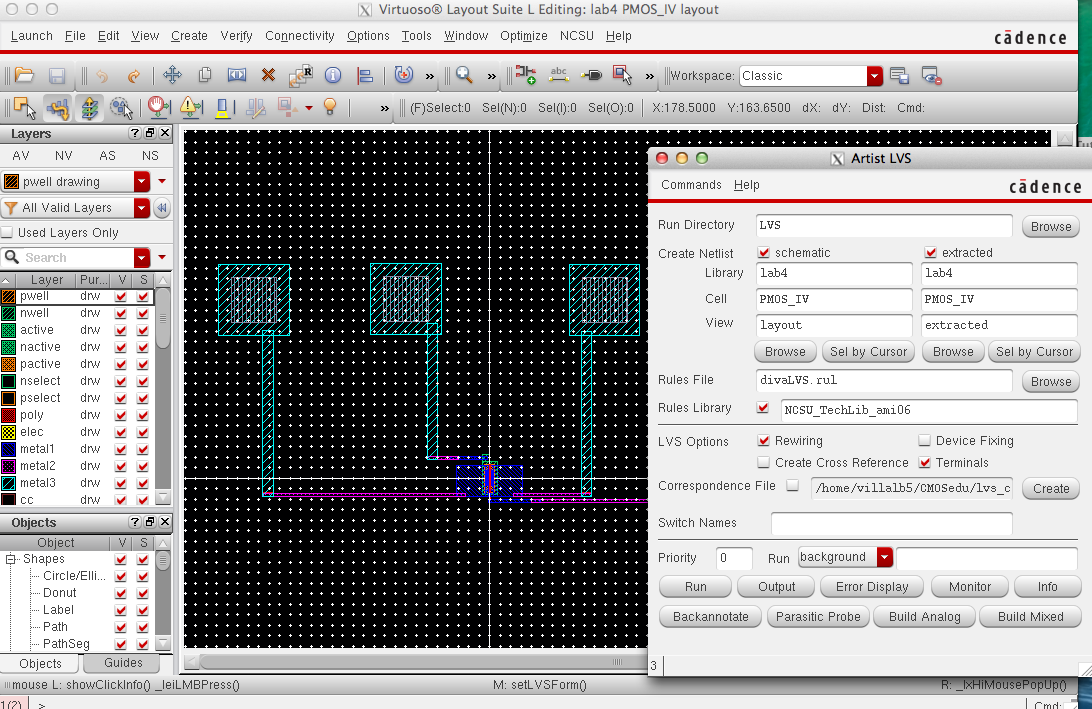
Now we have to create a layout for the NMOS and PMOS.Then perform a LVS and with a reference to a 4 pin NMOS and PMOS.
Here is the NMOS with one of the pins labeled as gnd! declaring it as a global which is tying the body to ground.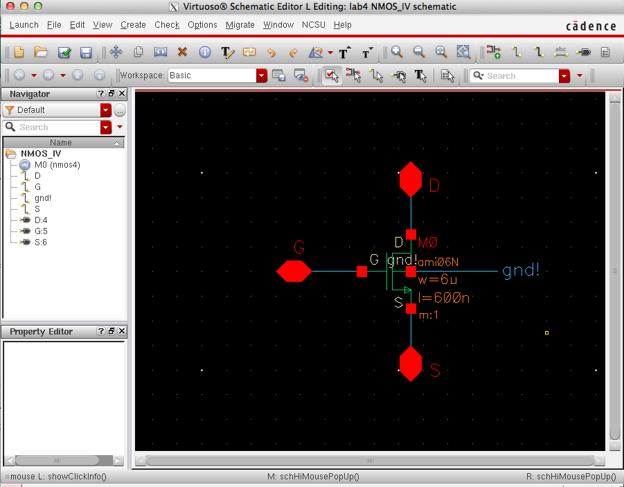
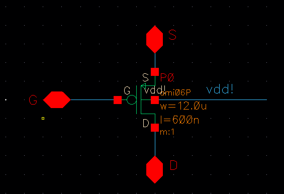
Now we will do the same for the PMOS
This now concludes lab 4. We now have a 4 terminal PMOS and NMOS
transistor complete with IV characteristics, schematics, layouts
including probe pad for testing.
Here you can download lab4.
Last thing to do is back up my work
Return to Michael Villalba's labs