Lab 3 - EE 421L
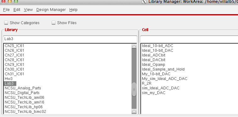
The first thing we need to do is copy all the cells from library Lab 2 into a new library that we will create called Lab3 so thatwe can compare results between the two.
Then we will need to create a layout cell called R_n_well_10k to create the 10k resistor.

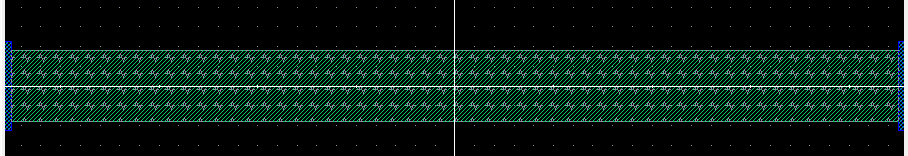
Once the layout opens create a rectangle using the n-well layer. (It doesnt matter how you lay it out because we will be making modifications to it.)
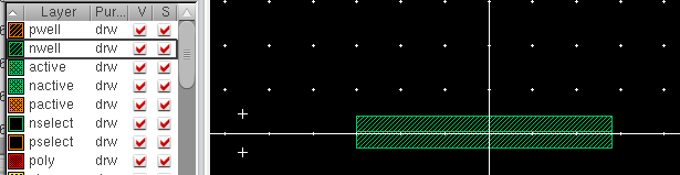
Now we need to make our modifications to our rectangle using the MOSIS design rules, because we are using the C5 process we will be using lambda as .3u (300nm). We also find from the design rules that there needs to be a minimum width of (12)lambda and a spacing of (18)lambda.
12xlambda = 3.6um
18xlambda = 5.4um
From the MOSIS sheet we see that the sheet resistance of a n-well is 800 squares.
To find a length and width that satisfies the design rules we can use the resistance formula to find our dimensions.
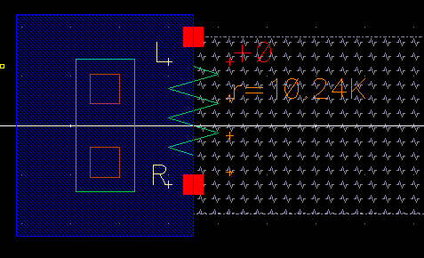
R = Rsquare *(L/W)
R= 10k, Rsquare = 800, and use W = 3.6um
Thus giving us L = 45um
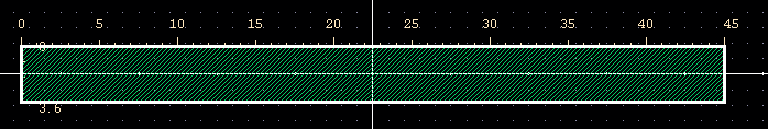
Now test to see if our parameters pass the DRC.
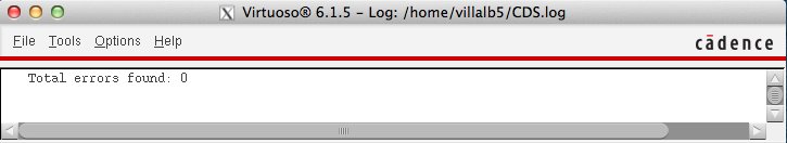
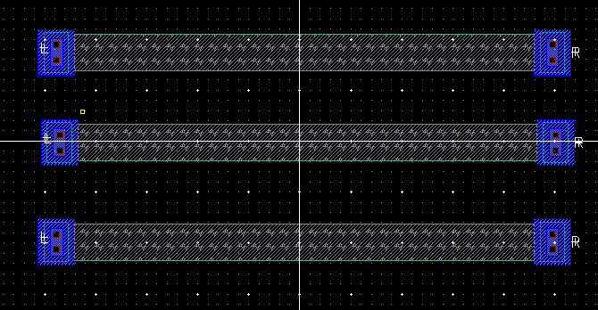
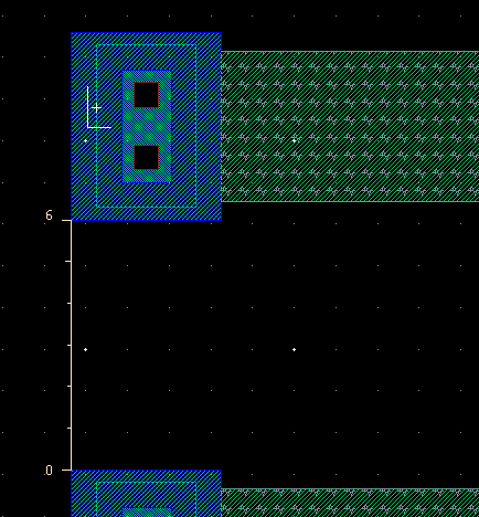
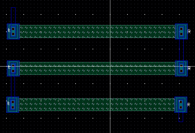
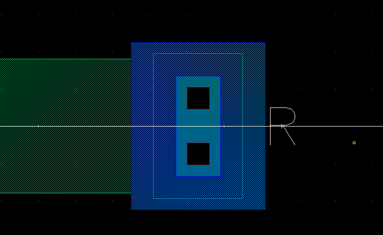
It does so we are okay to continue. We now need to add a n-tap on each end of the n-well rectangle. We can find n-tap in the NCSU_Techlib_ami06 and place on either side of the n-well.
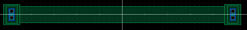
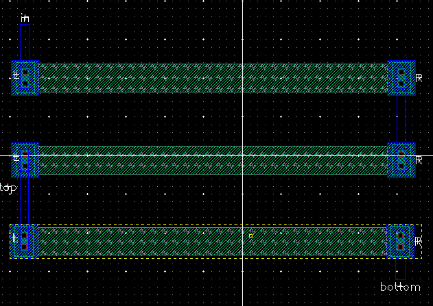
DRC once again to make sure there were no problems. Now we are going to add the pins at the end of the resistor to be connected. Choose metal 1 and create a pin over the n-tap giving the pin names L for metal1 that covers the left n-tap and repeat for the right n-tap.
Next DRC for no error issues. Now
we will need to place the final layer over the resistor. Select Res_id
and draw a rectangle that covers the n-well rectangle completely.