Lab 2 - EE 421L
Authored
by Mike Villalba villalb5@unlv.nevada.edu,
9-22-2014
PRELAB:
Download
lab2.zip to your desktop and then unzip the file into CMOSedu folder.
Then start Cadence library manager and go to sim_Ideal_ADC_DAC, open up
the schematic and launch an ADE simulation.
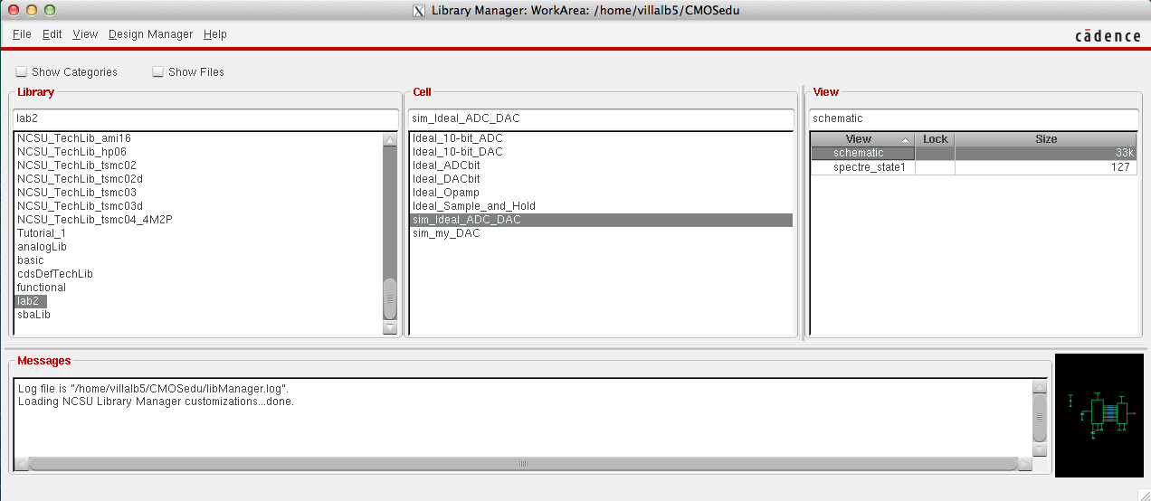
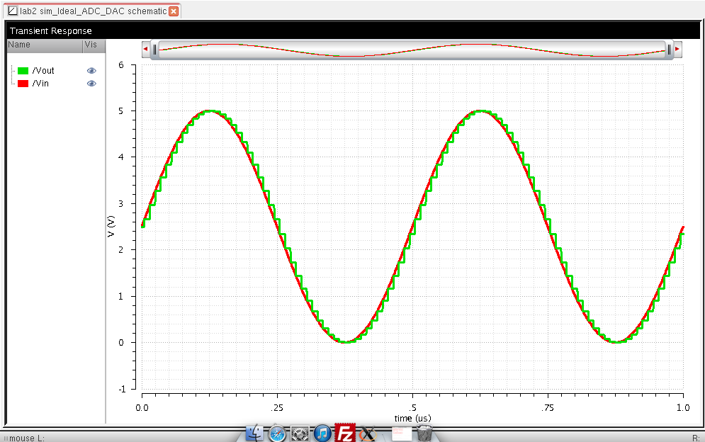
As show you have a discrete output and a smooth input.
LAB:
Create
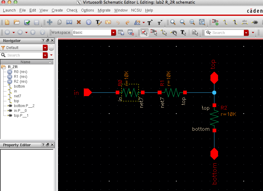
a new cell in the Lab2 library called R_2R and create a schematic. The
schematic should have two 10k Ohm resistors in series that will be
connected to a junction. There should be a top pin and another 10k ohm
resistor also connected to the junction. Then there should be a bottom
pin connected to the last resistor added.
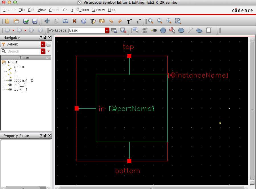
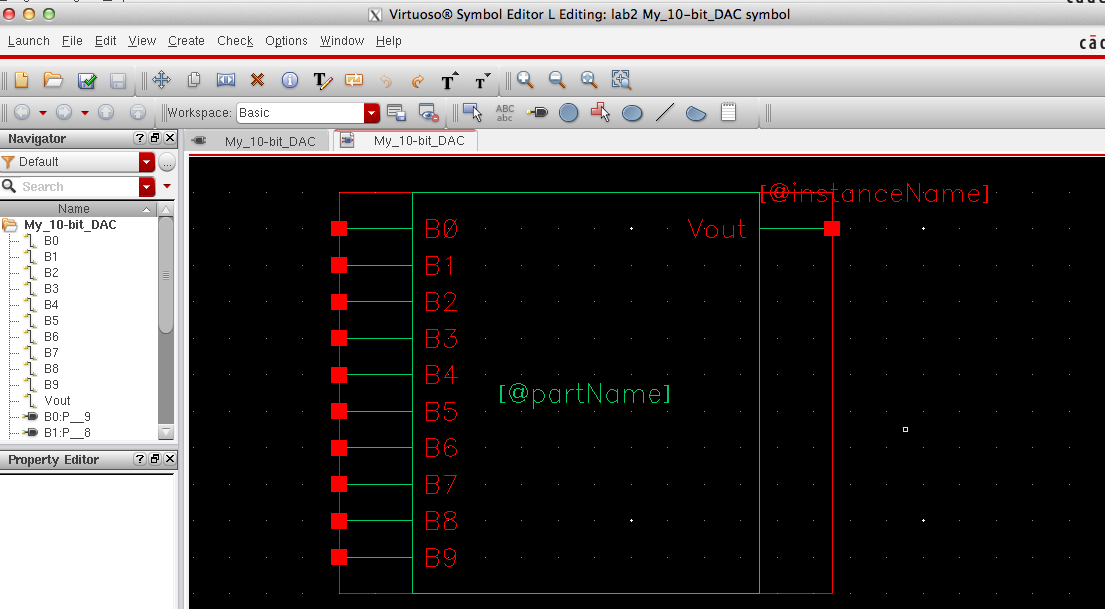
Next create a symbol for the R_2R schematic with the pins still being displayed.
I
then made a copy of the Ideal_10-bit_DAC and labeled it
My_10-bit_DAC. Onced I opened up the new copy of the
My_10-bit_DAC schematic I deleted everything in the schematic only
leaving the pins B0-B9. I then inserted the R_2R symbol that I
had created to the pins and connected a Vout pin to the the last B9
R_2R top pin while grounding the B0 bottom pin. After doing all this I
created another symbol named My_idealDAC.
I then connected My_idealDAC to the ADC.
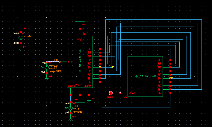
I
then tested it agian to make sure that I got the same outcome as before
to make sure that it worked. Then I tested the schematic
with a 10k resistor, which gave me a smaller amplitude on the
output due to the resistive load.
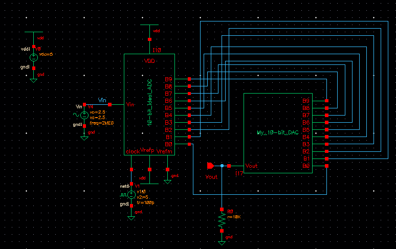
Then
I tested the schematic with a 10pF capacitor. This resulted in giving
me a smoother output than before with a time delay (0.7RC) being about
75ns.
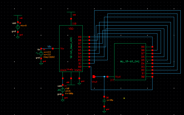
Last
thing I did was combined the 10k resistor and 10pF capacitor together
which resulted in a combination of the two previous test, smooth Vout
with a lower amplitude than Vin and a time delay.
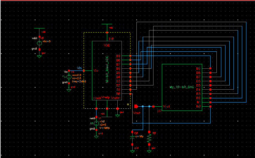
Having a higher resistance in the DAC will lead to a lower amplitude output with a longer time delay.
Here is evidence of me backing up my work.
Return to EE 421L Labs