Lab Project - EE 421L
Authored by Nick Repetti
repettin@unlv.nevada.edu
11/10/2014
Lab Description:
This lab will go over the design, layout, and simulation of an 8-bit ALU that can perform: A AND B, A OR B, A + B (addition), and A - B (subtraction).
Lab Report:
The first part of the lab will be the simulation the ALU. We have already done simulations for the following operations: AND, OR, ADD.
All that is left to design is the Subtracter and the logic to connect the parts of the ALU. Let's start with the Subtracter.
We could design a Subtracter from scratch, but there is a better way. We can take advantage of the fact that we already have an Adder.
In binary, subtraction is done by taking the 2's complement of the second number and adding it to the first. 2's complement is obtained by inverting all of the bits in a number and then adding 1 to it. The equation is found below.
A - B = A + B' + 1
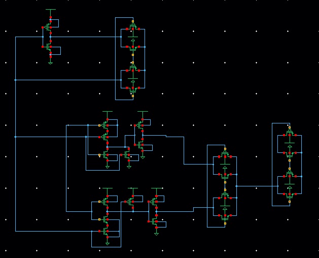
To implement this in our Adder, we simply Invert all of the bits of B and then set Cin = 1. We can use a 2-1 MUX to select whether the adder will perform addition or subtraction. The schematic can be seen below.
Adder/Subtracter
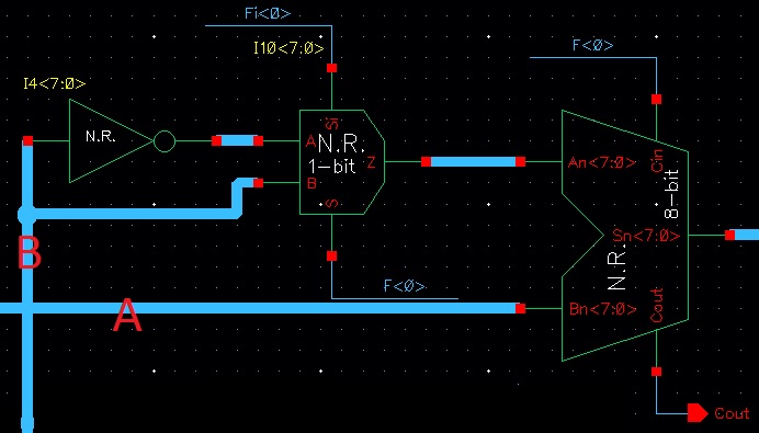
When F<0> = 0, B is selected from the MUX and then added to A with Cin = F<0> = 0. This is the Addition operation.
When F<0> = 1, B' is selected from the MUX and then added to A with Cin = F<0> = 1. This is the Subtraction operation.
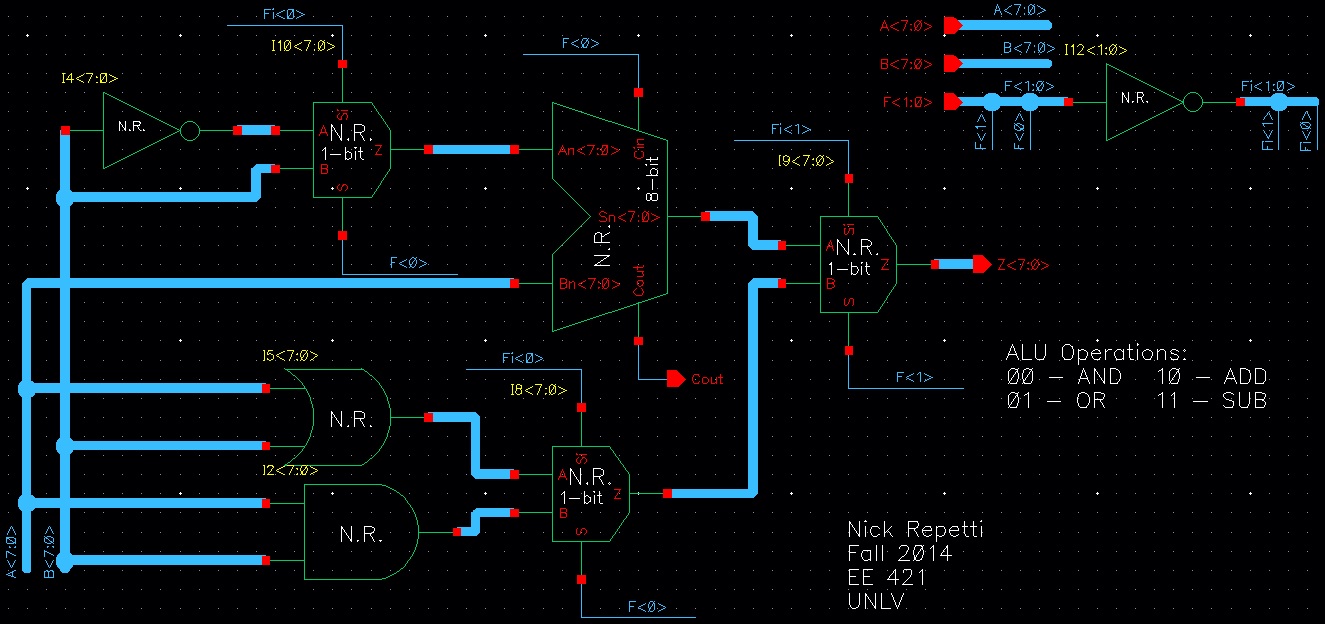
We now have all of the operations working correctly. Next up is to Design the ALU so that the F-bits will be able to select which operation to perform. We can use 2-1 MUXes chained together to get this result. The table below shows the operation of the ALU given the F bits.
| F1 |
F0 |
Operation |
| 0 |
0 |
AND |
| 0 |
1 |
OR |
| 1 |
0 |
ADD |
| 1 |
1 |
SUB |
Using this information, a schematic can be drafted using MUXes to connect the Symbols. The complete schematic for the ALU is seen below:
ALU Schematic:
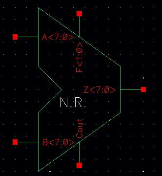
Now we can create a symbol for the ALU.
ALU Symbol:
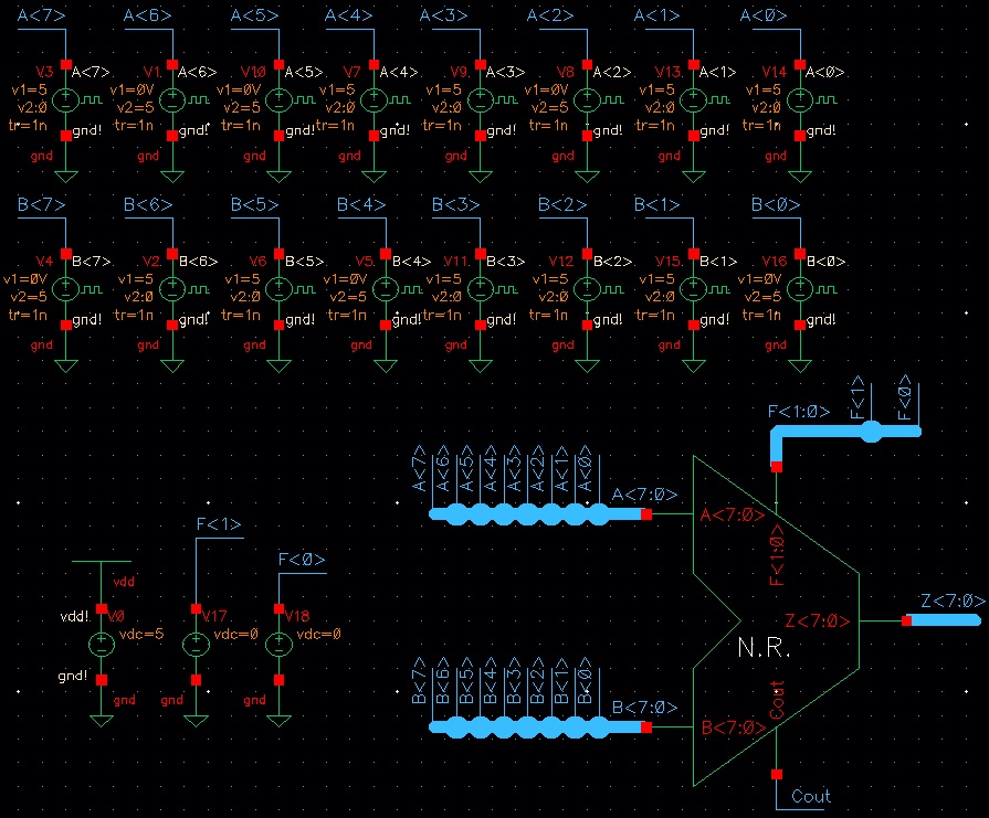
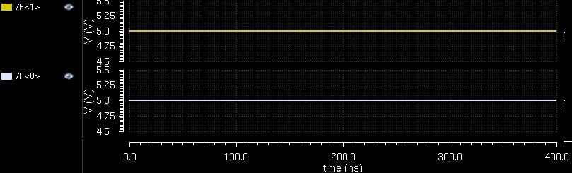
It is now time to simulate the ALU to verify that all of the operations are working correctly. We will do a Transient Simulation for 400ns on the schematic below. Note that A and B switch their values every 100ns so we can test 4 values in one plot:
ALU Simulation Schematic:
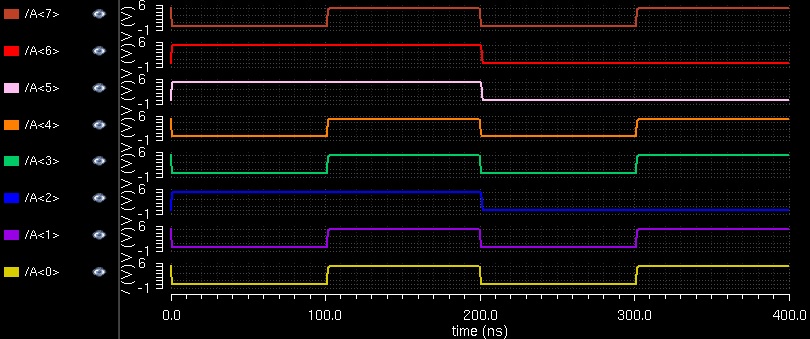
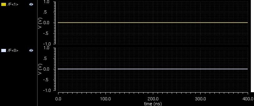
Below are the simulation results. Every operation was tested one at a time by changing the values of F<0> and F<1>. Note that A and B are the same for every simulation:
A:
B:
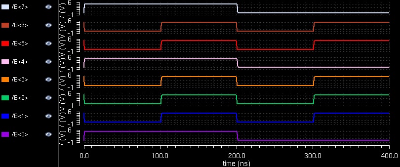
Let's begin with the AND Operation - 00:
AND - 00
AND - Results
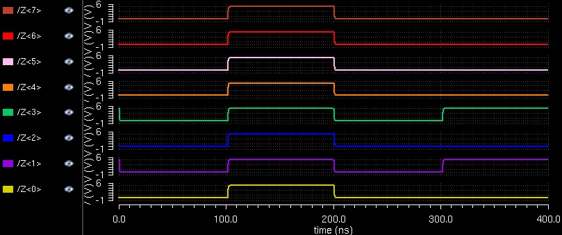
Looking at the data, the values for A and B change every 100ns, so that means there is a new output every 100ns.
Let's take a look at the data from 300-400ns:
A = 10011011
B = 01101110
Z = 00001010
All of the values are correct in the simulation. A AND B is confirmed to be working. Next let's look at the OR operation - 01:
OR - 01
OR - Results
Looking at the data, the values for A and B change every 100ns, so that means there is a new output every 100ns.
Let's take a look at the data from 0-100ns:
A = 01100100
B = 10010001
Z = 11110101
All of the values are correct in the simulation. A OR B is confirmed to be working. Next let's look at the ADD operation - 10:
ADD - 10
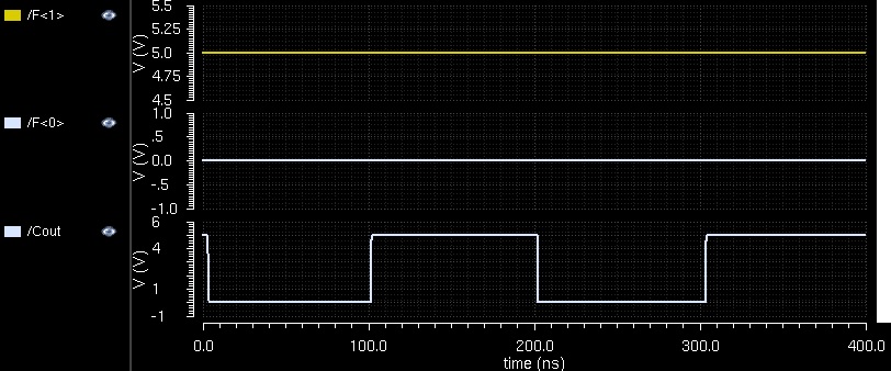
ADD - Results
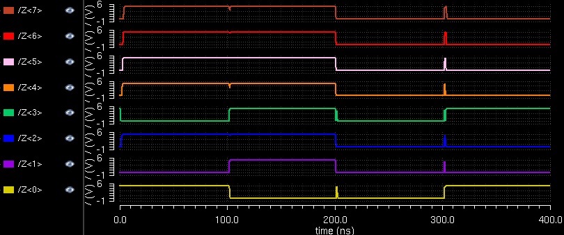
Looking at the data, the values for A and B change every 100ns, so that means there is a new output every 100ns.
Let's take a look at the data from 100-200ns:
A = 11111111 = 255 in decimal
B = 11111111 = 255 in decimal
255 + 255 = 510 in decimal = 111111110
Z = 11111110, but Cout = 1. We bring that bit down in front of Z to get 111111110 = 510 in decimal.
All of the values are correct in the simulation. A + B is confirmed to be working. Finally let's look at the SUB operation - 11:
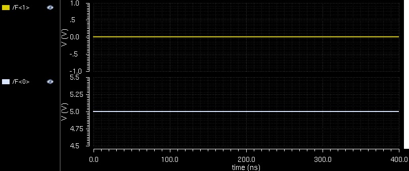
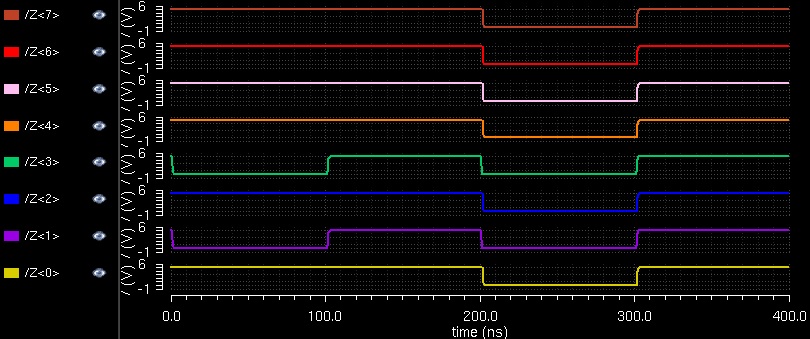
SUB - 11
SUB - Results
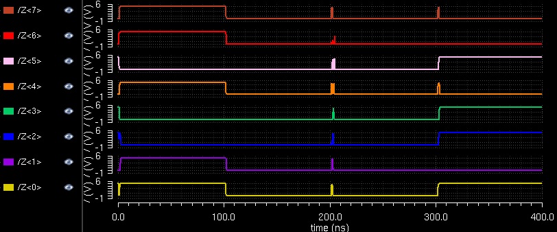
Looking at the data, the values for A and B change every 100ns, so that means there is a new output every 100ns.
Let's take a look at the data from 300-400ns:
A = 10011011 = 155 in decimal
B = 01101110 = 110 in decimal
155 - 110 = 45 in decimal = 00101101
Z = 00101010
Let's take a look at the data from 0-100ns to see what happens when we get a negative number:
A = 01100100 = 100 in decimal
B = 10010001 = 145 in decimal
100 - 145 = -45 in decimal = 11010011
Z = 11010011
All of the values are correct in the simulation. A - B is confirmed to be working. All operations are now confirmed to be working.
Part II - Layout
To start, I begin by using the 8-bit Full Adder layout from the previous lab. The 1-bit and 8-bit adders are seen below:
1-bit Adder
8-bit Adder
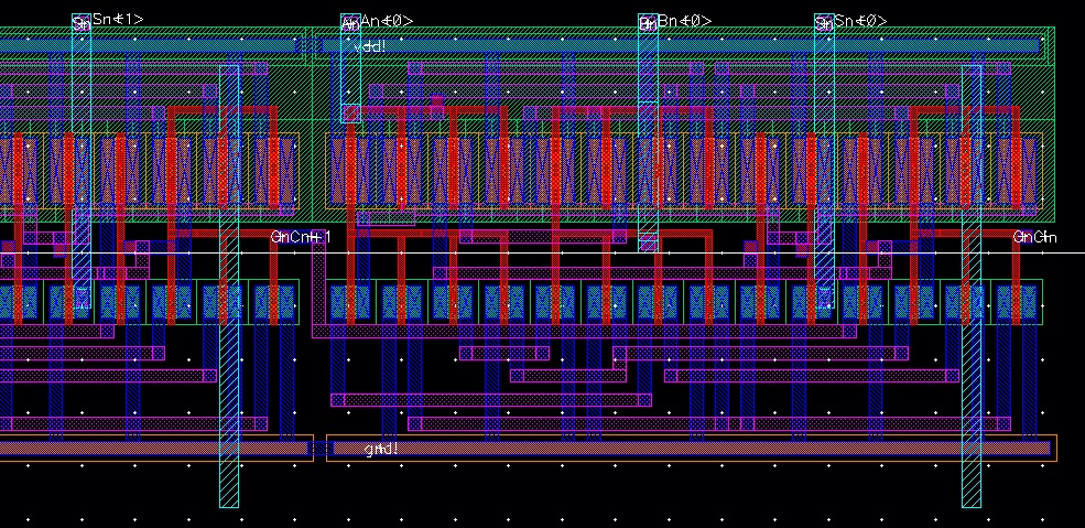
By using the adder cell as a template, I will design the rest of the ALU for 1-bit. The schematic and layout for 1-bit of the remaining is seen below:
Schematic:
Layout:
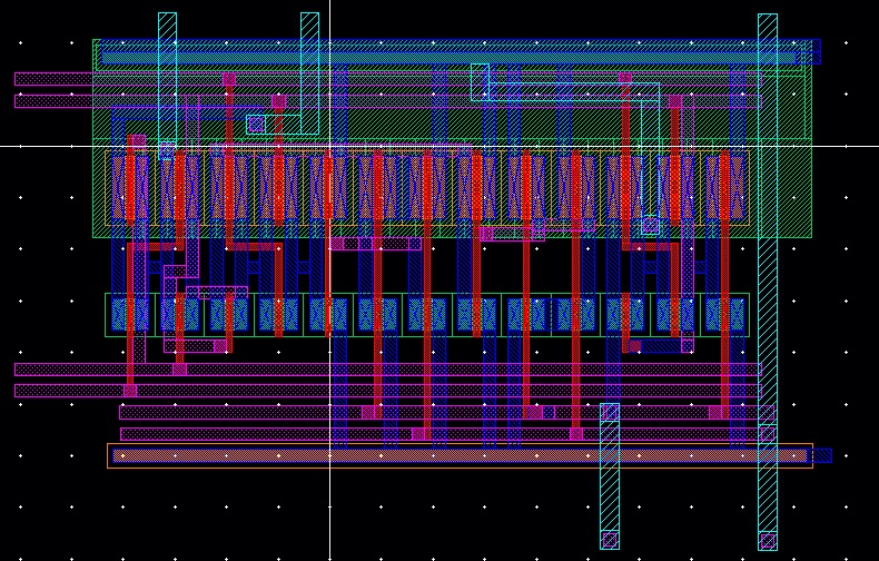
This cell will go on top of the adder. I flip it upside down so that the VDD rails are tied together. I then place them next to each other for all 8 bits just like the adder. The layout is seen below (Adder and Top portion):
Layout:
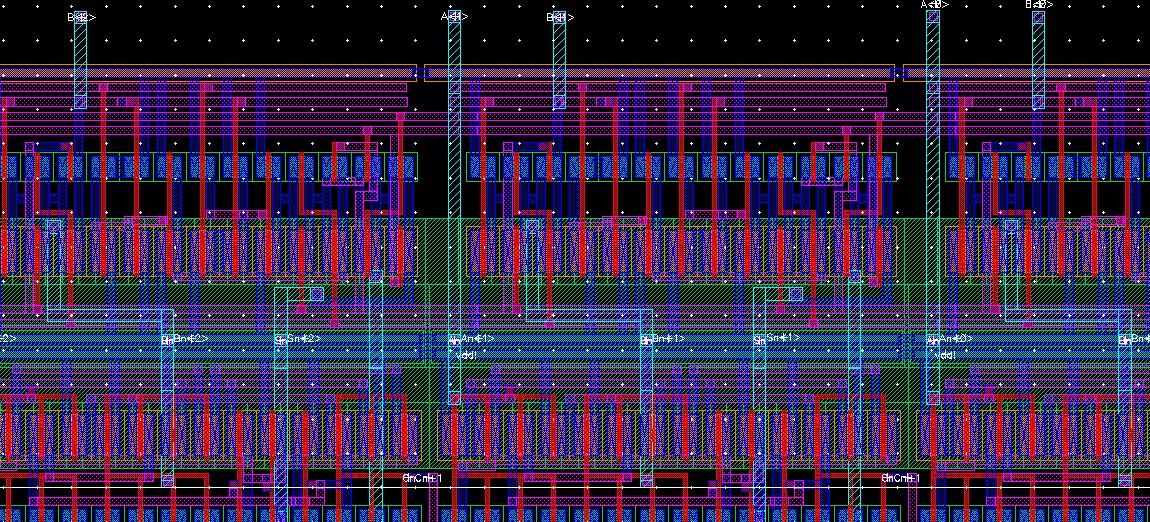
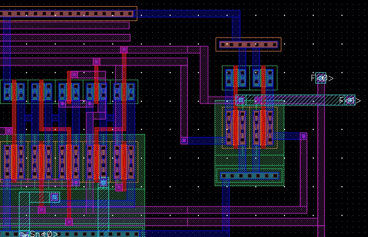
The last thing that needs to be added is the Inversion of the Select Bits. I then send all of the select bits to all 8-bits into the MUXs and Cin of the adder. This small portion is seen below:
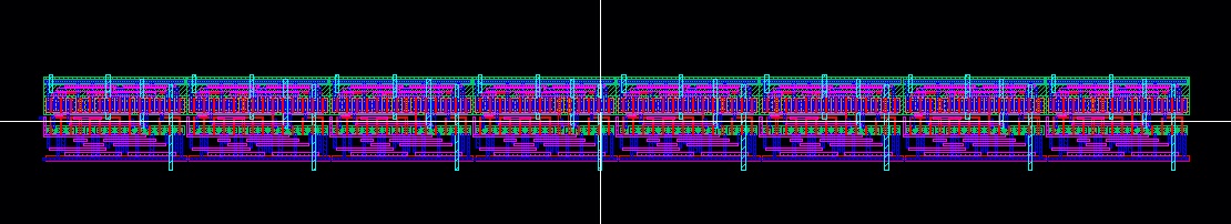
The final layout for the entire ALU is seen below:
ALU Layout (8-bits):
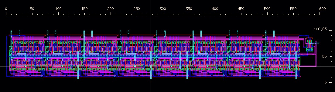
It is nice and compact and measures 600u x 100u which would fit easily into a chip.
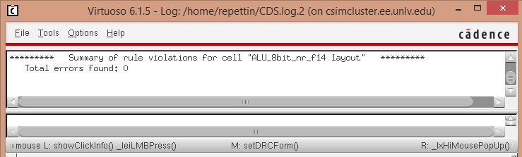
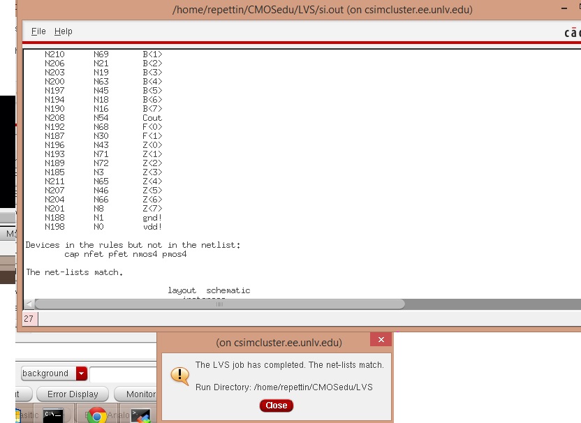
Finally I do a DRC and LVS to ensure that the entire thing is working properly. The results are seen below.
ALU Layout DRC:
ALU Layout LVS:
The lab is now complete. All of the work from this lab can be found in the zip file Lab_Project.zip
Back