
Lab Project - EE 421L
parke179@unlv.nevada.edu
The library for this Lab Project can be downloaded from the zip file located in this directory
http://cmosedu.com/jbaker/courses/ee421L/f14/students/parke179/project/other/
Direct download link
Part I: Designing and simulating the ALU
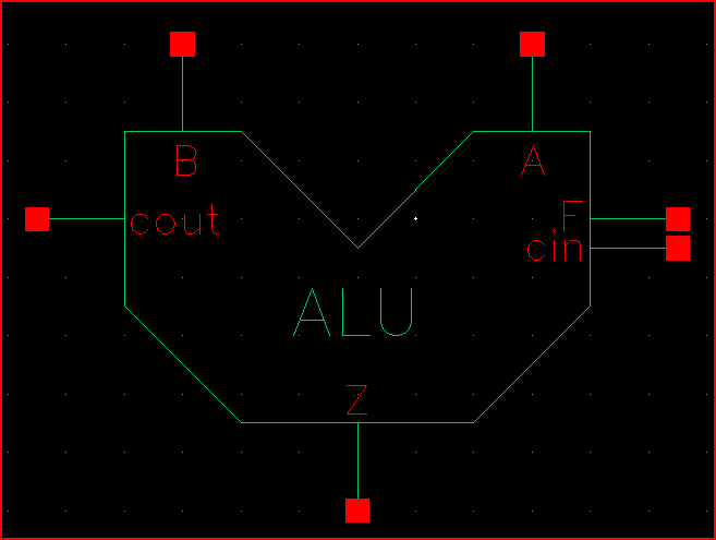
Figure 1 shows the final schematic for the 8-bit ALU.
Figure 1
Each component was created and tested in the earlier labs. The most complex component inside the ALU is the Full Adder.
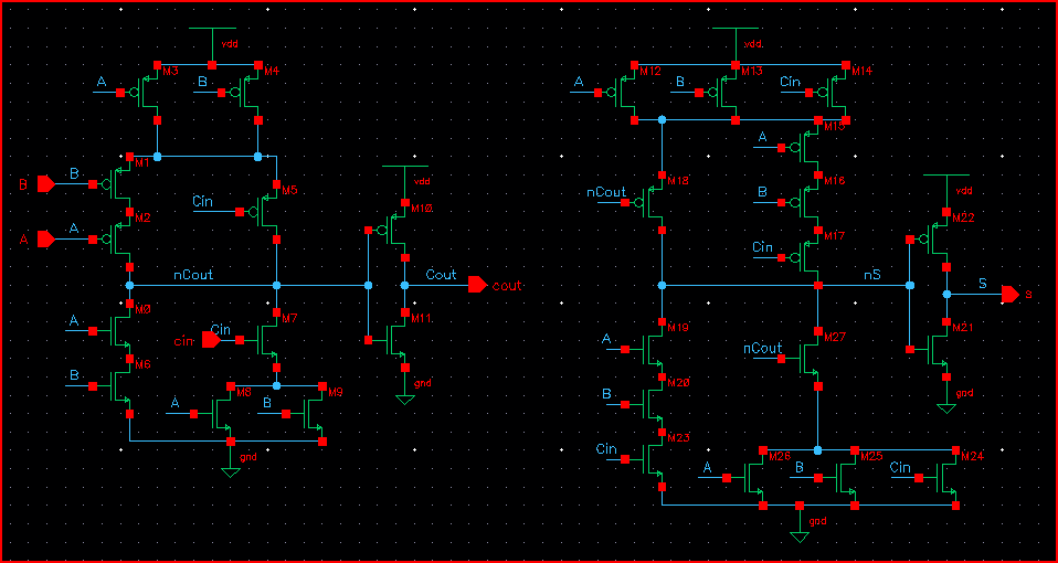
Figure 2 shows the schematic of the Full Adder. It uses fewer transistors than the simple schematic that uses XOR and NAND gates.
Figure 2
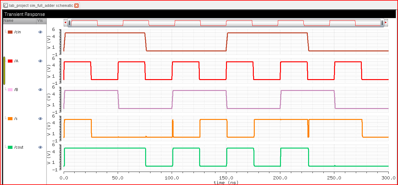
The simulation of the full adder is shown in figures 3a and 3b.
Figure 3a

Figure 3b
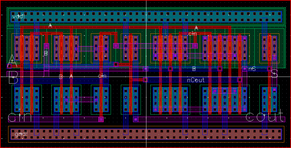
The layout of the full adder (figure 4) is much more compact than the version that uses XOR gates.
Figure 4
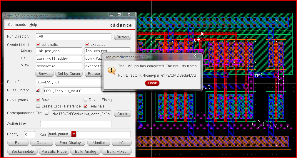
The layout should of course LVS.
Figure 5
Another major component of the ALU is the 2-to-1 multiplexer.
I have changed the MUX to only have 3 inputs by eliminating Si using an internal inverter.
Figure 5 shows the 2-to-1 MUX schematic.
Figure 5
After designing the MUX, I made a layout for it (figure 6).
Figure 6

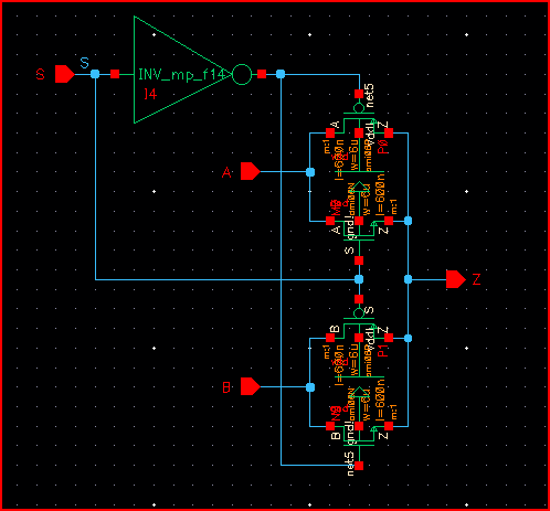
Before designing the 8-bit ALU, I made a 1-bit ALU symbol (figure 7) and schematic (figure 8).
Figure 7
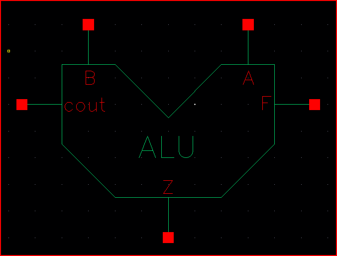
Figure 8: ALU schematic before updating MUXes

Figure 8 shows the 1-bit ALU design before updating the multiplexer to include an internal inverter.
The extra inverters that the change adds make the ALU not as efficient, but it will help simplify the schematic and layout.
The full adder uses F<1> and F<0> as the controls for deciding which function to perform. Table 1 lists the functions.
Table 1
|
F1 F0 |
Z |
|
00 |
A and B |
|
01 |
A or B |
|
10 |
A + B |
|
11 |
A - B |
The Full Adder is used as a Full Adder-Subtractor by allowing A-B. To perform A-B, it takes the two's compliment of B and performs A+(-B). The two's compliment is performed by inverting B and using 1 for the carry-in. F0 is set as Cin and the MUX input so that when F0=0 normal addition is done, and when F0=1 subtraction is done.
The carry-out from the full adder is set to be supressed when a non-addition function is performed by ANDing Cout with F1. When F1=1 there is an addition and Cout is shown. When F1=0, there is no addition so Cout is forced to zero.
The cascaded 2-to-1 MUXes create a 3-to-1 multiplexer to choose when to show the functions based on F from table 1.
Figures 9a and 9b show the simulation of the 1-bit ALU.
Figure 9a

Figure 9b
From the simulation in figure 9b, the value of Cout may seem strange. This is because Cout alone cannot be used to determine if the result is positive or negative. Extra logic would be needed to know when the result is negative or positive based on the value of A compared to B.
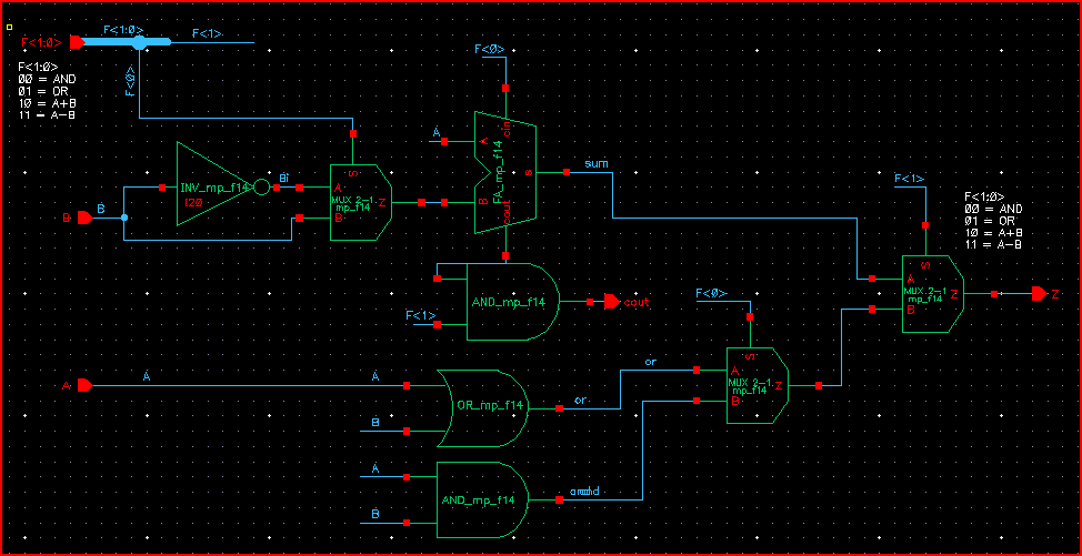
The schematic was remade using 3-input MUXes and the simulation was exactly the same.
Figure 10: 1-bit ALU with updated MUXes
After making a 1-bit ALU, each component is replaced with its 8-bit version to make an 8-bit ALU.
Figure 11
Figure 12

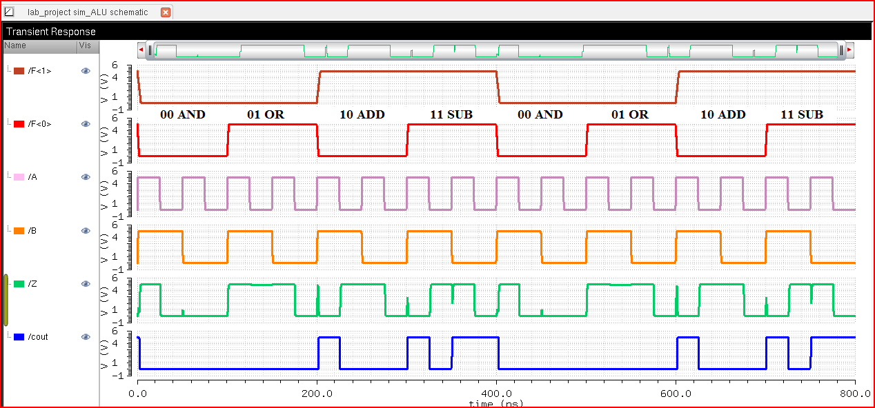
The simulation requires somewhat complex inputs in order to properly test it. Figure 13a shows the entire simulation, 13b shows AND function, 13c shows OR, 13d shows ADD, and 13e shows SUB.
Figure 13a: 8-bit simulation
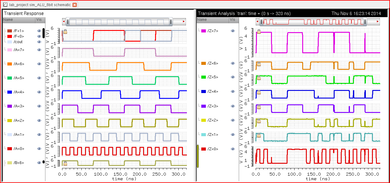
Figure 13b: 8-bit AND

Table 2: AND simulation
|
Time = |
0 to 40ns |
40ns to 80ns |
|
A = |
varies |
varies |
|
B = |
11111111 |
00000000 |
|
A and B = |
A |
00000000 |
Figure 13c: 8-bit OR

Table 3: OR simulation
|
Time = |
80ns to 120ns |
120ns to 160ns |
|
A = |
varies |
varies |
|
B = |
11111111 |
00000000 |
|
A or B = |
11111111 |
A |
Figure 13b: 8-bit ADD
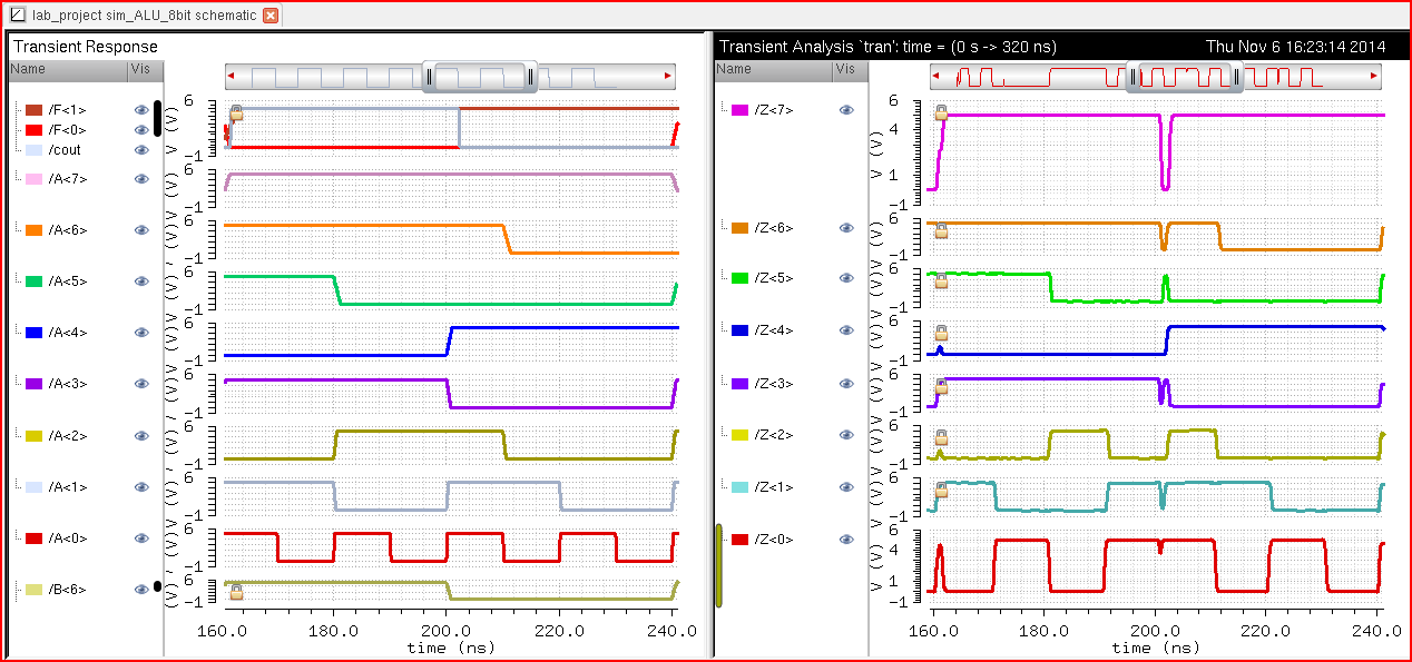
Table 4: ADD simulation
|
Time = |
160ns to 170ns |
… |
180ns to 190ns |
… |
200ns to 240ns |
|
A = |
11101011 |
… |
11001101 |
… |
varies |
|
B = |
11111111 |
… |
11111111 |
… |
00000000 |
|
A + B = |
11101010 |
… |
11001110 |
… |
A |
|
Cout = |
1 |
… |
1 |
… |
0 |
Figure 13e: 8-bit SUB
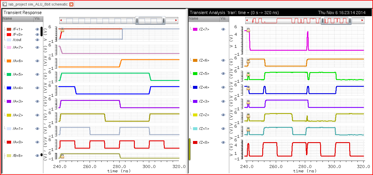
Table 5: SUB simulation
|
Time = |
240ns to 250ns |
250ns to 260ns |
… |
280ns to 320ns |
|
A = |
00111111 |
00101110 |
… |
varies |
|
(-B) = |
00000001 |
00000001 |
… |
00000001 |
|
A - B = |
01000000 |
00101111 |
… |
A+1 |
|
Cout = |
0 |
0 |
… |
1 |
All of the results match the expected values.
Part II: Laying out the ALU
Before laying out the entire ALU, it is a good idea to plan ahead.
The 8-bit ALU schematic shown in figure 11 earlier used an 8-bit version of each component (such as full adder, multiplexer, AND gate, etc). Doing the layout this way would require 8-bit layouts for every component, and then several 8-bit wire busses to route and connect.
Another way to make an 8-bit ALU is to use eight 1-bit ALUs. In order to use a 1-bit ALU this way, it must have an additional export pin for Cin. Figures 14a and 14b show the schematic of the ALU module.
Figure 14a: Modular ALU schematic

Figure 14b: Modular ALU Symbol
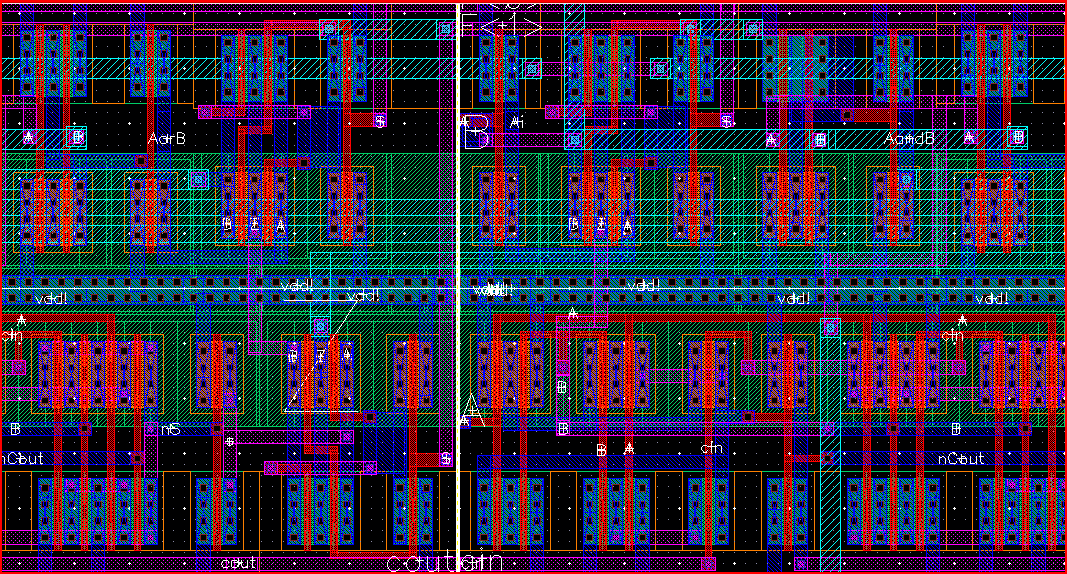
To make the ALU compact, each component was updated so that it has the same standard pad frame. In other words, VDD and GND were made to match the size of the Full Adder and the NMOS and PMOS were alligned as well. Figure 15a shows the laayout of a 1-bit ALU module. This layout will be used to make a modular 8-bit ALU.
Figure 15a: Layout of 1-bit ALU module
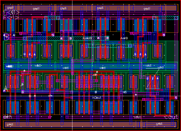
The ALU is somewhat complicated, so each component is annotated and labeled in figure 15b
Figure 15b: Annotated ALU
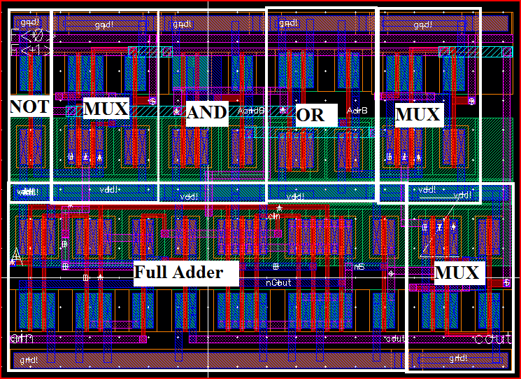
From planning ahead, I made sure that the Cout would allign with the Cin of the next ALU, and that the function selection bits, F<1> and F<0>, would allign too. The only tricky output will be the Z for each ALU, so the label for it was made large enough to see while zoomed out.
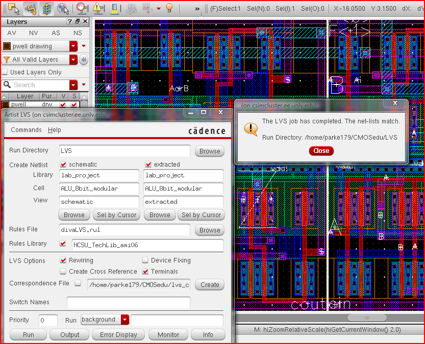
Before moving on to the 8-bit layout, this 1-bit ALU should LVS.
Figure 16:

Figure 17 shows the schematic for the modular 8-bit ALU. It uses the 1-bit ALU module that has a Cin.
This circuit was simulated and had the same results as the regular 8-bit ALU that uses 8-bit components.
Figure 17

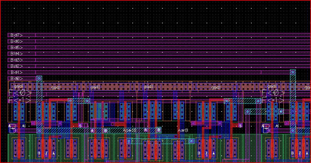
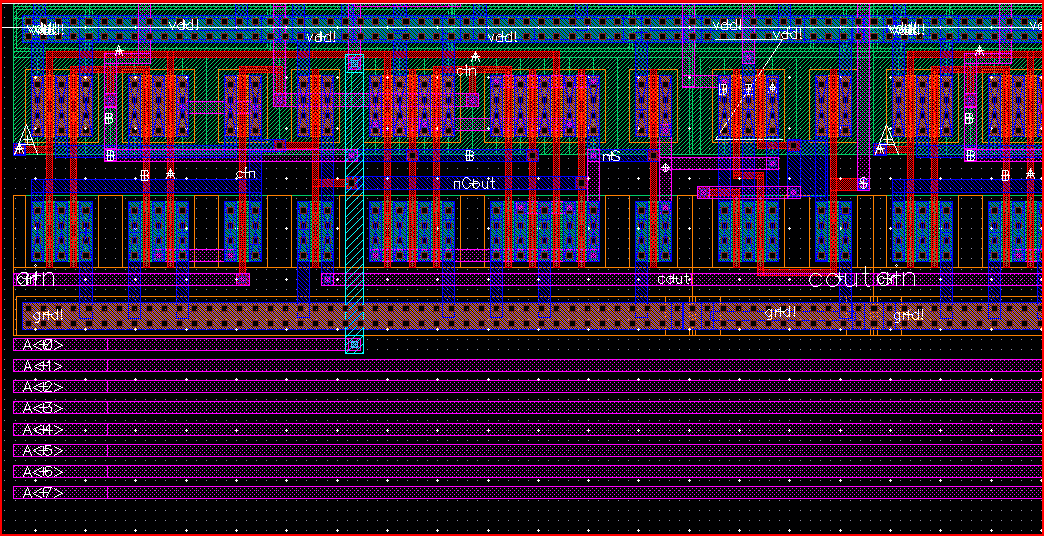
The entire 8-bit ALU is shown in figure 18.
Figure 18a: 8-bit ALU lauyout

The B inputs are on the top left.
Figure 18b: 8-bit ALU lauyout top left.
The A inputs are on the bottom left.
Figure 18c: 8-bit ALU lauyout bottom left
The Z outputs and Cout are on the right. In order to get the Z outputs there took some careful routing.
Figure 18d: 8-bit ALU lauyout right

The ALUs are perfectly alligned and have VDD and GND bridges between them.
Figure 18e: 8-bit ALU lauyout two ALUs connecting
The modular 8-bit ALU is ran through a LVS to see if it matched the modular schematic.
Figure 19a: modular LVS
As a bonus, the layout is ran through LVS to see if it matches the non-modular ALU schematic.
This schematic is fundamentally different in design, and yet the layout is still identical, which means either 8-bit ALU design will have the same result.
Figure 19b: non-modular LVS

Backups
While the project was in progress, I made several backups to ensure that I would not lose data in case of an accident. I also made several changes to older components, so I kept the older backups just in case I needed to revert them back.

The library for this Lab Project can be downloaded from the zip file located in this directory