Lab 08 - EE 421L
Authored
by Matthew Parker, Ting Yu, and Leanna Guevara
parke179@unlv.nevada.edu , yut2@unlv.nevada.edu , guevaral@unlv.nevada.edu
December 1, 2014
Lab
description: The goal of this lab is to make a layout that is ready for
fabrication under the MOSIS c5 process. This is a group project.
Group Members' course directories:
Matthew Parker
Tiny Yu
Leanna Guevara
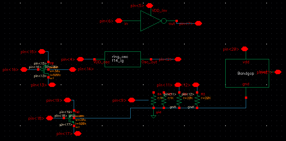
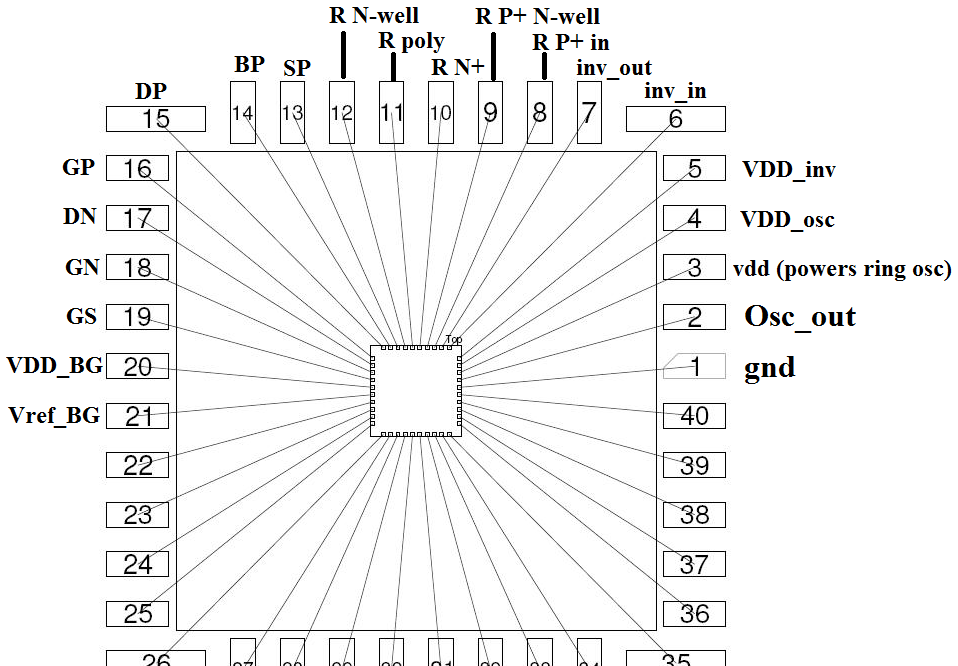
Devices included in test chip:
- 30u/0.6u NMOS (3 pins, DN, GN, SN, connect the p+ body, B, of the NMOS to the chip's ground pin)
- 30u/0.6u PMOS (4 pins, DP, GP, SP, and BP)
- Inverter made using 30u/0.6u NMOS and 60u/0.6u PMOS (3 pins, in, out, VDD_inv)
- 61 stage ring oscillator using 6u/0.6u MOSFETs with off-chip buffer (2 pins, VDD_osc and Ocs_out. Ground connected to pin 20)
- 20k n-well resistor (2 pins)
- 20k hi-res poly resistor (2 pins)
- 1k n+ resistor (2 pins)
- 1k
p+ resistor (3 pins, need n-well to isolate the p+ from the p-substrate
and the n-well needs to be tied to a voltage >= either side of the
resistor)
- Bandgap reference (2 pins, VDD_bg and Vref)
Part I: Layout
The Schematic is shown in Figure 1.
Figure 1
In
order to LVS, the N+ and P+ resistors must be excluded. They will still
be in the layout, but Cadence is unable to identify them (even with
R_id).
Figure 2: Schematic for LVS
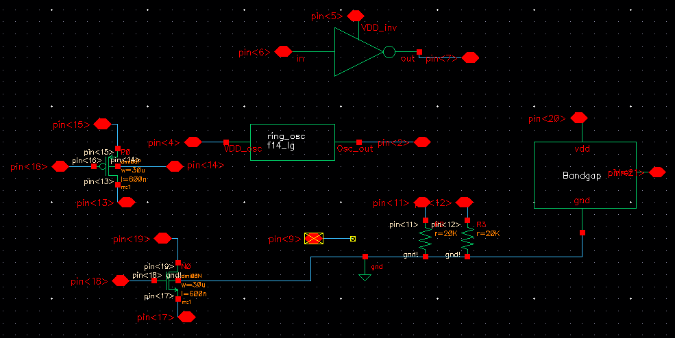
Figure 3 shows layout.
Figure 3
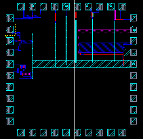
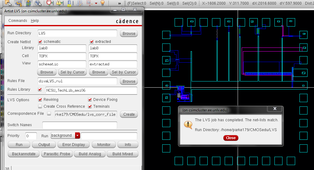
Figure 4 shows LVS
Figure 4
Part II: Testing
When fabricated chip comes in the components need to be checked seperately to ensure that the design fuctions properly.
- 30u/0.6u NMOS (3 pins, DN, GN, SN)
| Pin | Connected to | Reads |
| DN | 5V (VDD) | |
| GN | 0V | |
| SN | | 5V |
- 30u/0.6u PMOS (4 pins, DP, GP, SP, and BP)
| Pin | Connected to | Reads |
| DP | | 5V -> 0V |
| GP | 0V -> 5V | |
| SP | 5V | |
| BP | 5V | |
- Inverter made using 30u/0.6u NMOS and 60u/0.6u PMOS (3 pins, in, out, VDD_inv)
| Pin | Connected to | Reads |
| In | 0V->5V | |
| Out | | 5V ->0V |
| Vdd_inv | 5V | |
- 61 stage ring oscillator using 6u/0.6u MOSFETs with off-chip buffer (2 pins, VDD_osc and Ocs_out. Ground connected to pin 20)
| Pin | Connected to | Reads |
| VDD_osc | 5V | |
| Osc_out | | Frequency |
- 20k n-well resistor, 20k hi-res poly resistor, 1k n+ resistor (2 pins)
Measure the resistance between both ends, resistance should be close to what is in the layout- 1k
p+ resistor (3 pins, need n-well to isolate the p+ from the p-substrate
and the n-well needs to be tied to a voltage >= either side of the
resistor)
Connect the n well to 5V and then measure the resistance between the remaining pins.
- Bandgap reference (2 pins, VDD_bg and Vref)
| Pin | Connected to | Reads |
| VDD_bg | 5V | |
| Vref | | 1.25V |
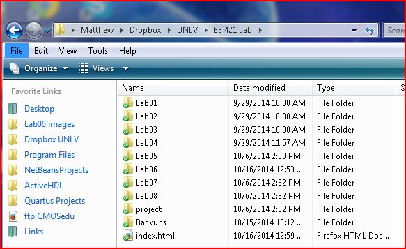
Creating backups
Dropbox was used to backup all screenshots, project files, and html files. I
do so by using the dropbox folder as my active work area to save to,
and then dropbox automatically uploads changes to the files.
The library for this Lab08 can be downloaded from the zip file located in this directory
http://cmosedu.com/jbaker/courses/ee421L/f14/students/parke179/Lab08/other/
Direct download link