Lab 07 - EE 421L
Authored
by Matthew Parker
parke179@unlv.nevada.edu
October 26th, 2014
Lab
description: The goal of this lab is to create all the components needed to make an 8-bit full adder.
The library for this Lab07 can be downloaded from the zip file located in this directory
http://cmosedu.com/jbaker/courses/ee421L/f14/students/parke179/Lab07/other/
Direct download link
Part I: Using busses to make multi-bit gates
Tutorial
5 covers how to make a ring oscillator using busses. Figure 1 shows the
schematic of a ring oscillator and figure 2 shows the simulation
results.
Figure 1: Ring Oscillator
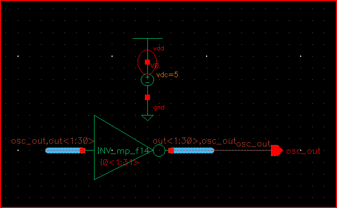
Figure 2: Ring oscillator simulation

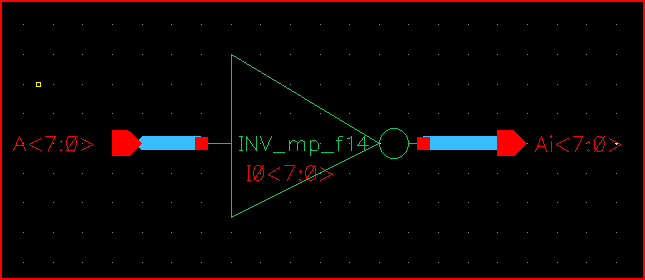
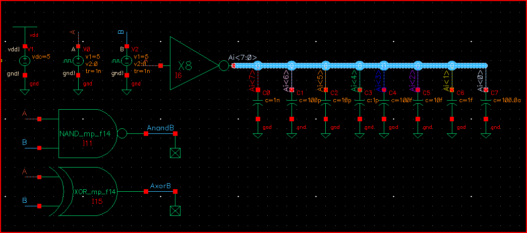
Making an 8-bit inverter uses busses in a similar way, except they are in parallel instead of in series like a ring oscillator.
The
simulation of the 8-bot inverter will use capacitors to show that the
output has a rise time when attached to a capacitive load.
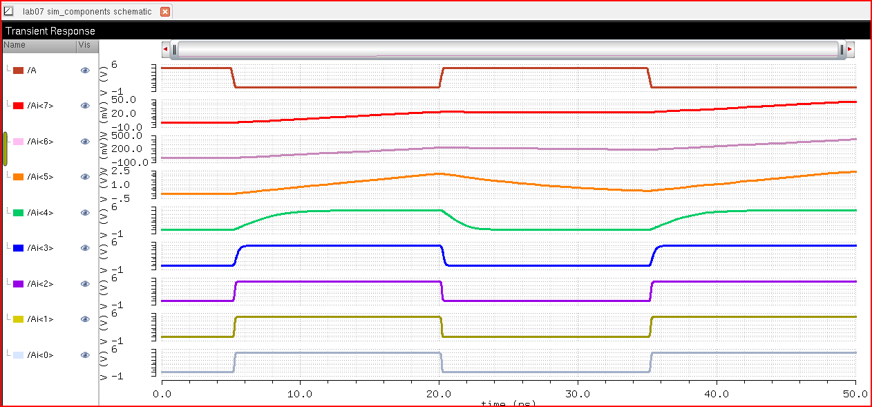
There are two types of delay, Tplh for propagation low to high, and Tphl for high to low.
Tplh = 0.7Rp(Cout + Cload)
Tphl = 0.7Rn(Cout + Cload)
Where:
Rn = R'n L/W = 15k/10 = 1.5k
Rp = R'p L/W = 45k/10 = 4.5k
Cout = C'ox (WnLn + WpLp) = 2.5fF(10+10) = 50f
For large values of Cload (100pF or more), the value of Cout is insignificant and the delay equals:
Tplh = 0.7(1.5k)Cload = 105ns for 100pF
Tphl = 0.7(4.5k)Cload = 315ns for 100pF
At 1pF (output Ai<4>),
Tplh = 0.7(1.5k)(1.05p) = 1.1025ns
Tphl = 0.7(4.5k)(1.05p) = 3.3075ns
At 100fF (output Ai<3>),
Tplh = 0.7(1.5k)(150f) = 0.1575ns
Tphl = 0.7(4.5k)(150f) = 0.4725ns
At 500fF,
Tplh = 0.7(1.5k)(550f) = 0.5775ns
Tphl = 0.7(4.5k)(550f) = 1.7325ns
After
simulating the 8-bit inverters, I repeated the simple steps to make an
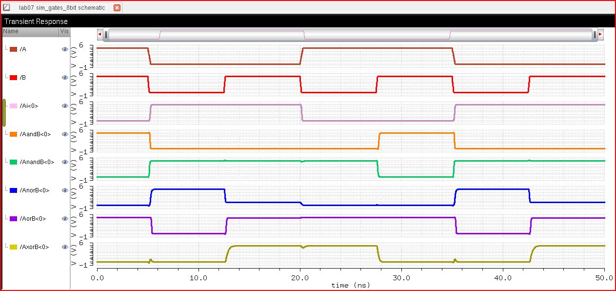
8-bit version of a NAND, AND, NOR, OR, and XOR gate.
The AND/OR gates are simply a NAND/NOR gate with an inverter at the end.
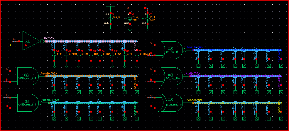
All
of the inputs will be tied together, so the simulation will only show a
single output for each 8-bit gate, since they are all identical.
Part II: Making an 8-bit 2-to-1 MUX/DEMUX
Figure 10 shows the schematic of a 2-to-1 multiplexer.
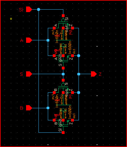
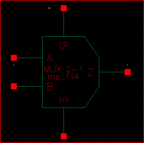
The circuit can be used as a MUX or DEMUX. Figure 12 shows the configuration for MUX mode.
A and B are inputs, while Z is the output.
Figure 12: 2-to-1 MUX
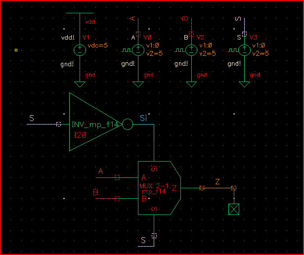
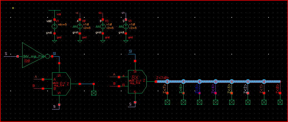
After verifying it works as a 1-bit circuit, I used the same process as earlier to make it an 8-bit MUX.
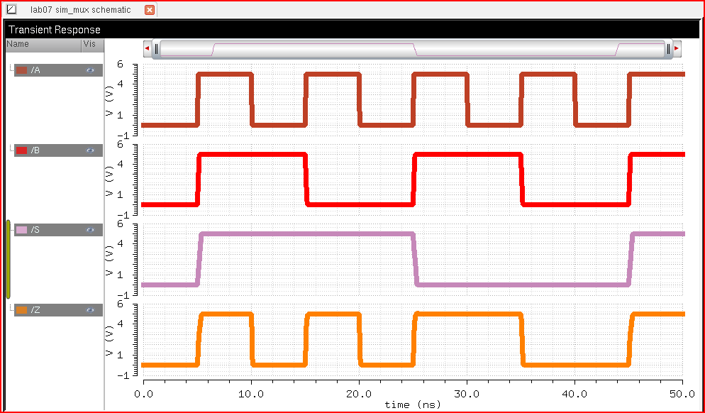
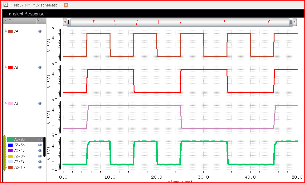
Figure 14 shows the 8-bit 2-to-1 MUX with A and B as inputs and Z as output.
Figure 14: 8-bit 2-to-1 MUX
Only a single output is shown since they are all identical when the inputs are equal.
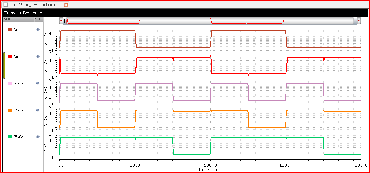
Another use of the MUX is as a DEMUX.
Figure 16 shows the DEMUX configuration where Z is the input and A and B are the outputs.
Figure 16: 8-bit 1-to-2 DEMUX
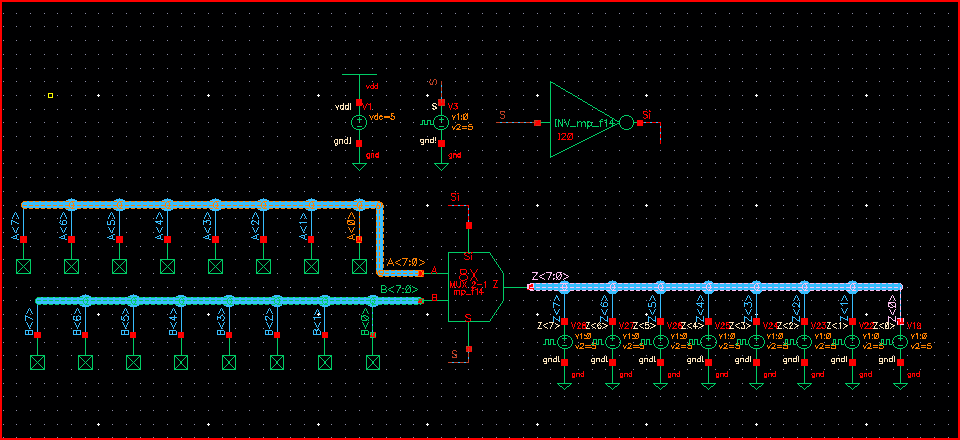
Figure 17 shows the output in DEMUX mode. Z is the input while A and B are outputs.
Figure 17: DEMUX simulation
Part III: Making an 8-bit Full Adder
The final component of an ALU is the full adder. A single full adder is cascaded to make an 8-bit full adder.
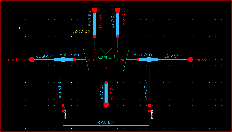
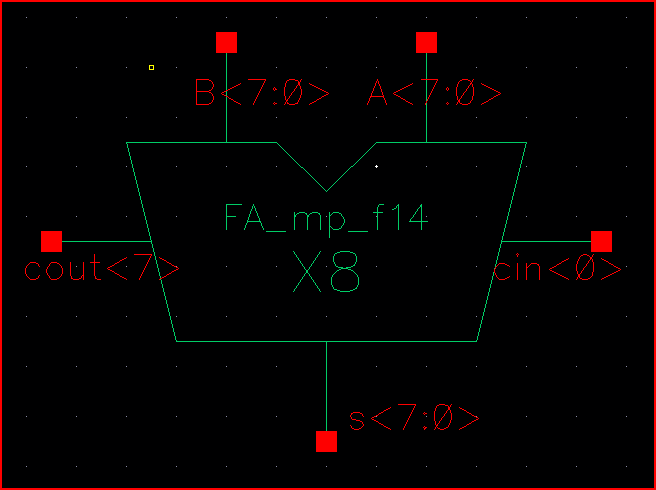
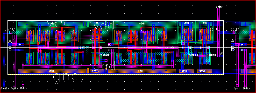
Figure 20 shows the left-most full adder in the layout of the entire 8-bit full adder.
The Cin<0> of the first FA is the only Cin that does not come from a previous FA.
The metal-2 recangles uses for A, B, Cin<1:7>, and Cout are copies along with the FA in an array of 8 collumns.
Figure 20: 8-bit FA left
The only other special FA is the last FA, which has the final output pin Cout<7>.
Figure 21: 8-bit FA right
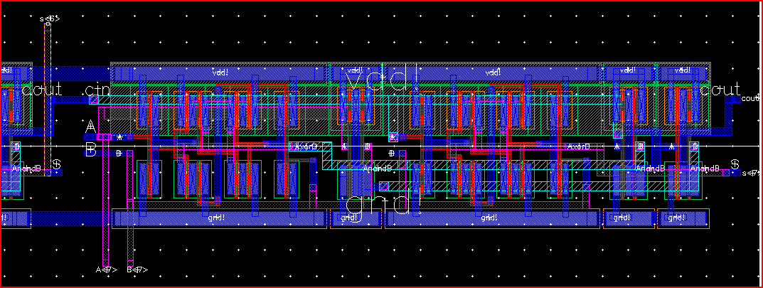
Figure 22: 9-bit FA layout
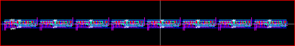
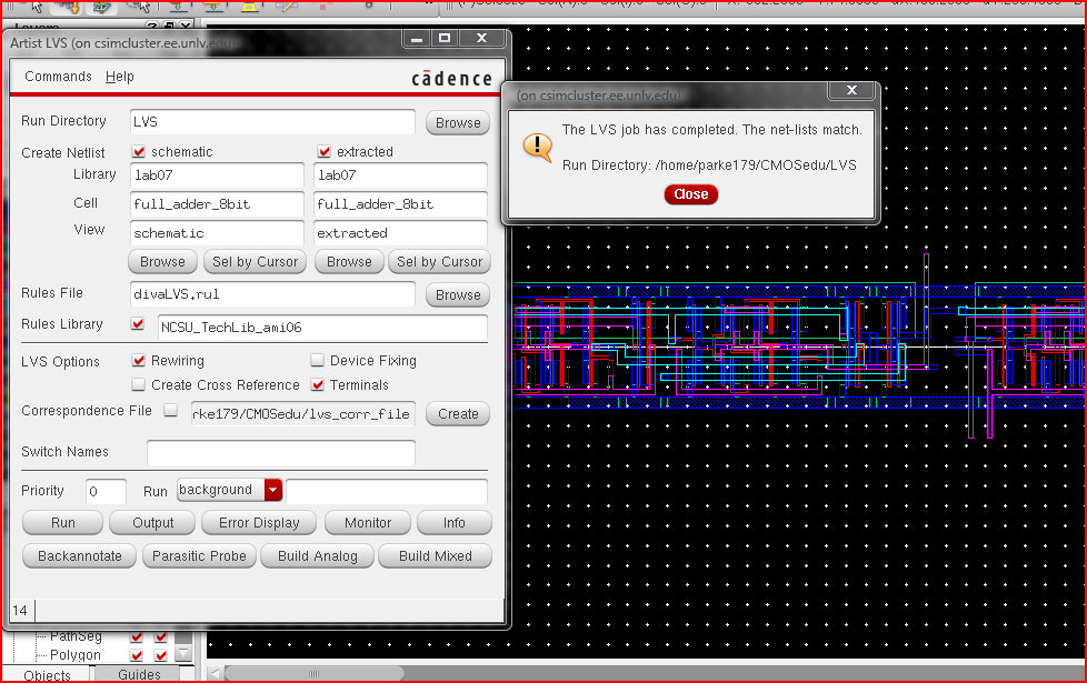
An LVS is ran and succeeds.
To test the 8-bit FA, the inputs A<7:0> and B<7:0> vary slightly and Cin<0> is a simple pulse.
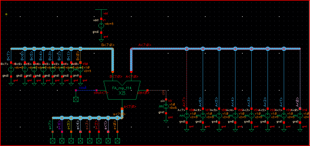
Figure 25: 8-bit FA sim
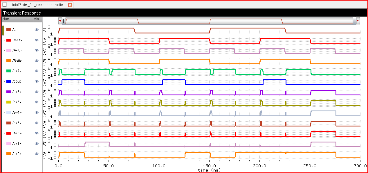
Figure 25 shows the simulation of the 8-bit FA.
Inputs A<0> to A<6> are all the same pulse voltage, and A<7> is a pulse with double the period of the others.
B<0> is a pulse function with the same period as A<7>, and B<7:1> are all a constant 0 volts.
There are glitches in the FA's output whenever A<6:0> transition, but they last less than a nano second.
Table 1 summarizes some of the results from the simulation in figure 25.
Table 1: Results of 8-bit FA sim
|
|
0-25ns
|
25-50ns
|
50-75ns
|
...
|
250-275ns
|
275-300ns
|
|
Input A
|
11111111
|
10000000
|
01111111
|
...
|
01111111
|
00000000
|
|
Input B
|
00000001
|
00000001
|
00000000
|
...
|
00000000
|
00000000
|
|
Input Cin
|
1
|
1
|
1
|
...
|
0
|
0
|
|
|
|
|
|
|
|
|
|
Output S
|
00000001
|
10000010
|
10000000
|
...
|
01111111
|
00000000
|
|
Output Cout
|
1
|
0
|
0
|
...
|
0
|
0
|
Creating backups
I
use dropbox to backup all screenshots, project files, and html files. I
do so by using the dropbox folder as my active work area to save to,
and then dropbox automatically uploads changes to the files.
The library for this Lab07 can be downloaded from the zip file located in this directory
http://cmosedu.com/jbaker/courses/ee421L/f14/students/parke179/Lab07/other/
Direct download link