Lab 06 - EE 421L
parke179@unlv.nevada.edu
The library for this Lab06 can be downloaded from the zip file located in this directory
http://cmosedu.com/jbaker/courses/ee421L/f14/students/parke179/Lab06/other/
Direct download link
Part I: Making the NAND gate
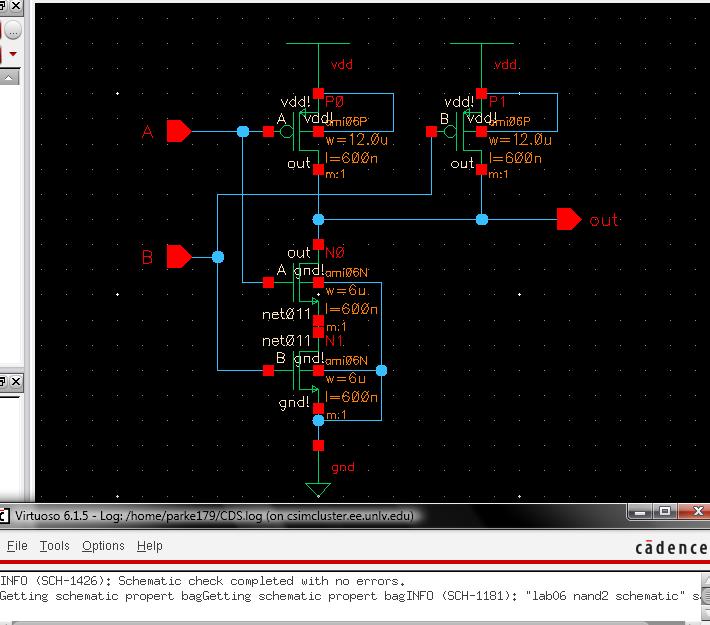
Figure 1 shows the schematic of the NAND gate. The NMOS' pull the output to zero when both inputs are high, and the PMOS' pull the output to vdd when at least one output is low.
Figure 1: Schematic of NAND
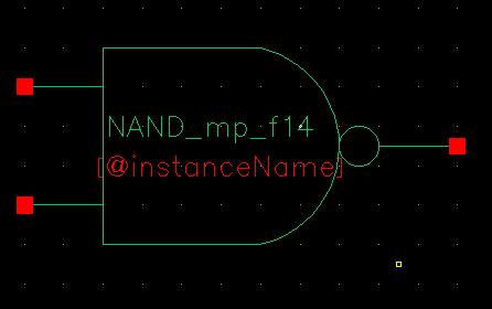
The symbol used is the same as the one provided by Dr. Baker located here.
After making the schematic, the next step is to lay it out. I modified the inverter from the previous lab, making sure to change the size of the PMOS to 6u (even though it is not as good as a 12u/6u gate).
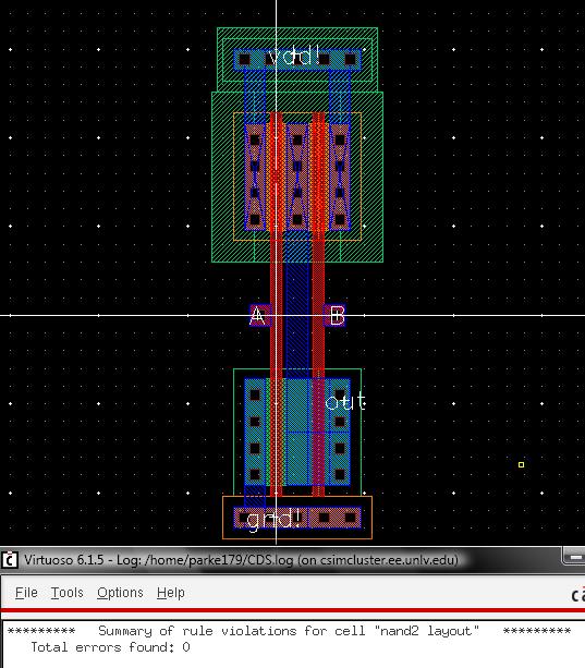
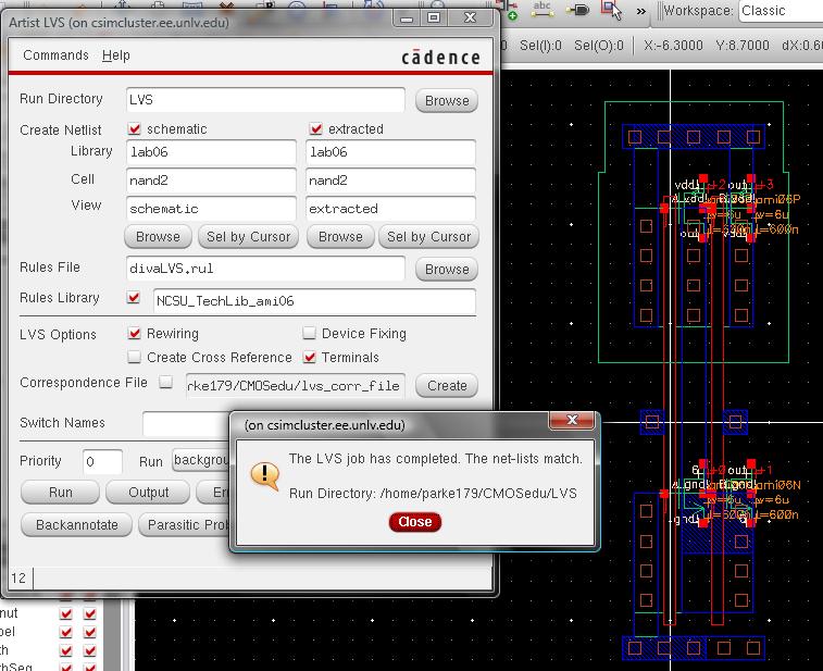
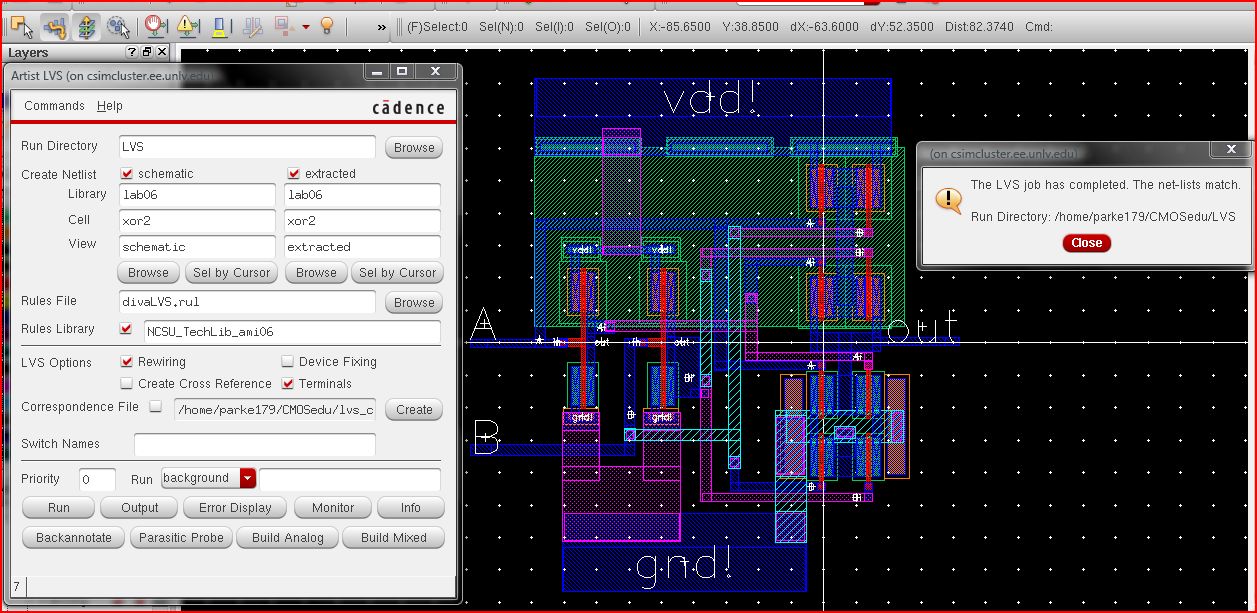
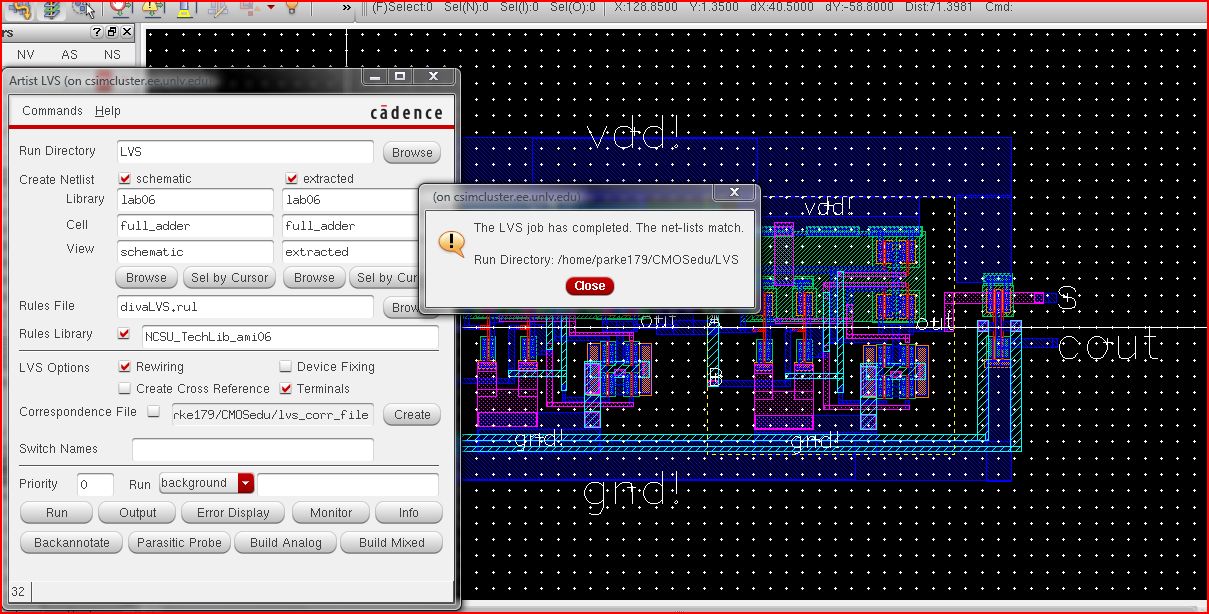
After extracting the layout, an LVS is performed.
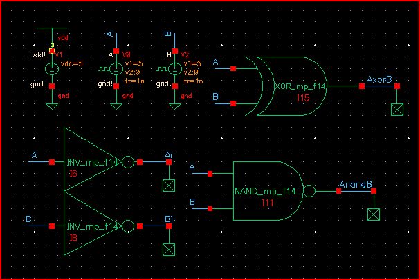
The simulation is done in a schematic that tests mutliple simple components. Later on, the XOR gate will be added.
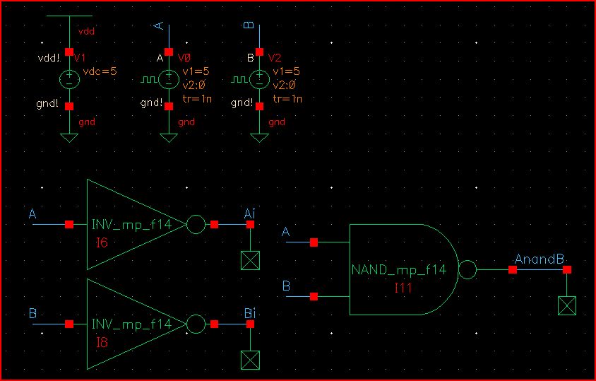
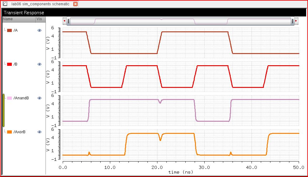
Figure 6 shows that the NAND gate is low when both inputs are high, and high otherwise.
Figure 6: Simulation of NAND gate and inverter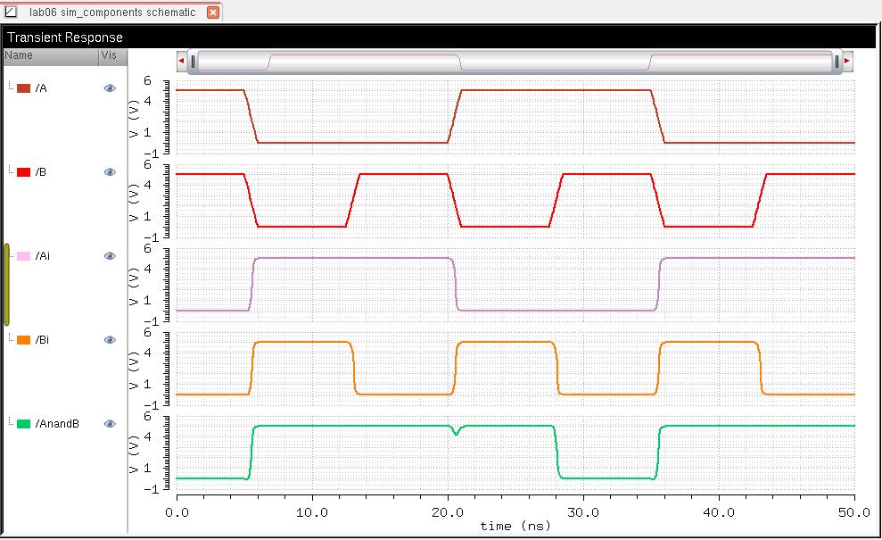
Part II: Making the XOR gate
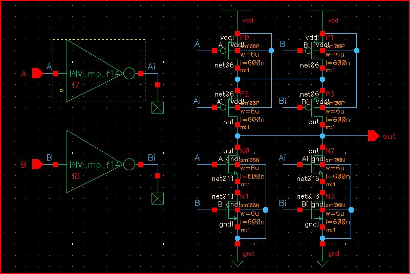
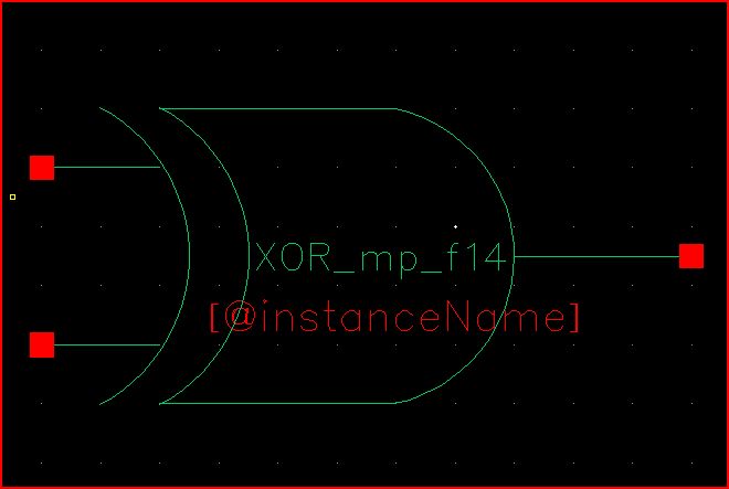
Figure 7 the schematic of the XOR gate. The inverters have been updated to be 6u/6u is both layout and schematic (and a LVS confirmed it is correct).
Figure 7: XOR schematic
One special thing to be aware of, is that having a 4-way intersection of wires causes a warning.
This warning is called a solder dot warning, and it happens because when a circuit is printing, the dot dissapears, making it unclear if it is a 4-way intersection or just two wires crossing each other. A 3-way intersection is allowed because it is less ambiguous.
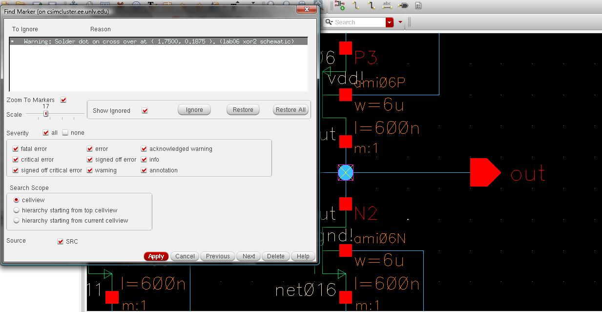
The warning can be ignored and the schematic will still work.
To prevent the message from appearing in the future, add this script into your .cdsinit file located in your CMOSedu lab directory.
; Disable warning for a 4-way interesection wire aka solder dot crossover
envSetVal("schematic" "srcSolderOnCrossover" 'cyclic "ignored")
; ------
The symbol used is the same as the one provided by Dr. Baker located here.
The XOR gate is simulated in the same schematic used to simulate other small components.
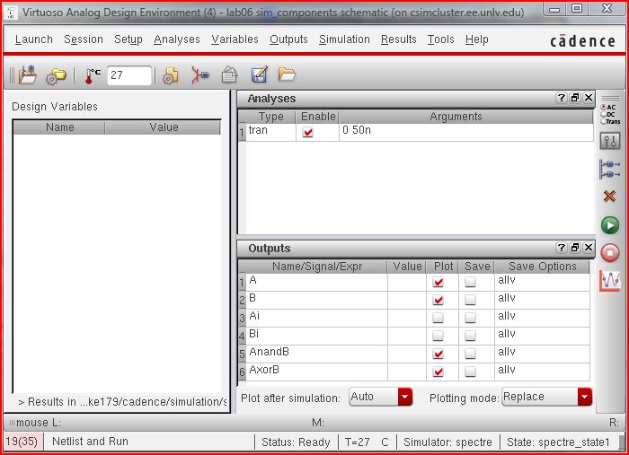
After setting the ADE to not plot Bi and Ai, the simulation of the XOR gate shows that it is high when exactly one input is high.
The glitches in the output are caused by having both inputs change at the same time, which causes a delayed propagation through the smaller components in the XOR gate.
After simulation, the next step is to layout the XOR gate. My design isn't as compact as it could be, but it still works.
Figure 13: Layout of XOR gate
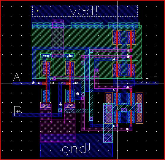
Figure 13 shows the entire layout of the XOR gate. Figures 14 and 15 show the upper-right corner and lower-right corner of the schematic, which have 4 PMOS' and 4 NMOS', respectively.
Figure 14: Upper-right corner showing the 4 PMOS'
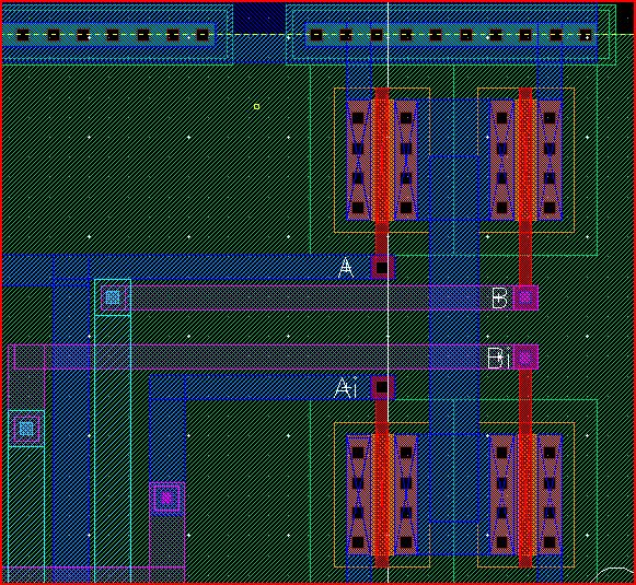
Figure 15: Lower-right corner showing the 4 NMOS'
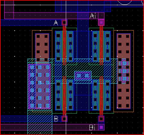
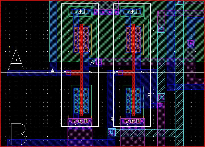
Figure 16 shows that the inverters made in the previous lab (and modified to be size 6u/6u) were instantiated into the layout.
After the layout is finished, we run an LVS and hope that it works.
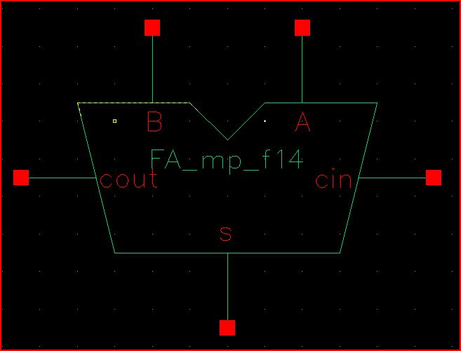
Part III: Making the Full Adder
The final part of this lab is to use the components made earlier to make a full adder.
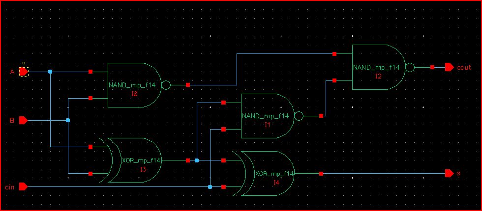
The symbol used is the same as the one provided by Dr. Baker located here.
The simulation will be done in a seperate schematic from the smaller components.
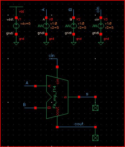
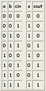
Figure 21 shows the simulation of the Full Adder. It matches the expected outputs in Figure 21b.
Figure 21: Simulation of Full Adder

Figure 21b: Truth table for full adder (source: Dr. Baker)
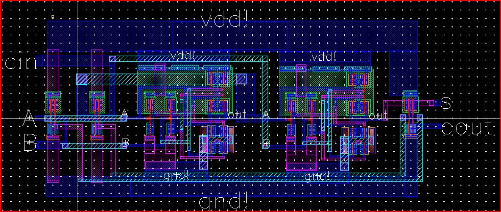
The last step is to layout the full adder and perform an LVS.
Creating backups
I use dropbox to backup all screenshots, project files, and html files. I do so by using the dropbox folder as my active work area to save to, and then dropbox automatically uploads changes to the files.
The library for this Lab06 can be downloaded from the zip file located in this directory