Lab 04 - EE 421L
parke179@unlv.nevada.edu
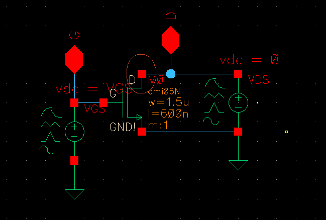
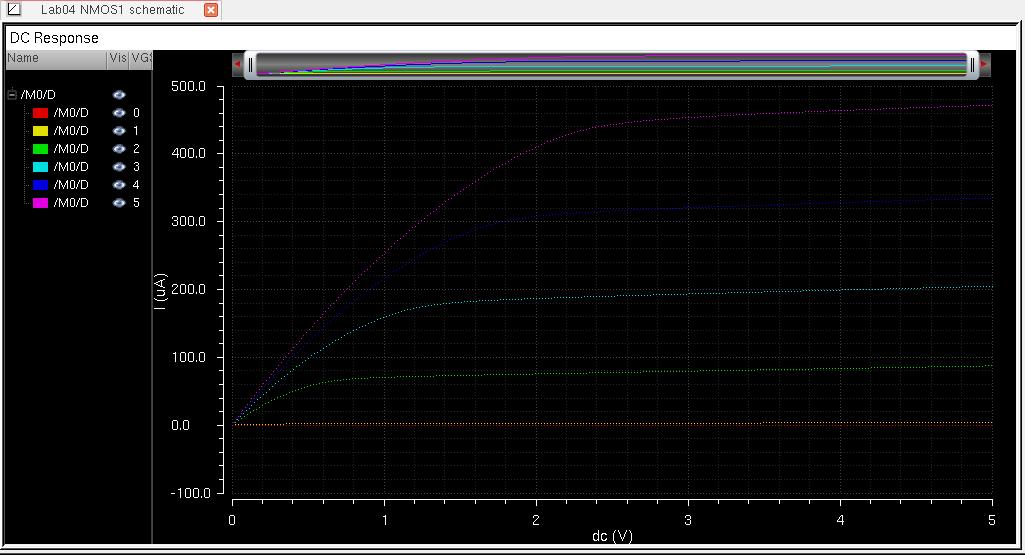
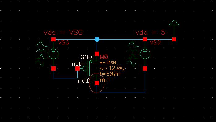
Part I: NMOS ID vs VDS
VGS varies from 0 to 5 V in 1 V steps and VDS varies from 0 to 5 V in 1 mV steps.
The simulation shows ID vs VDS at different values of VGS.
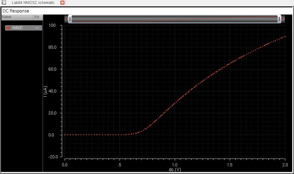
Part II: NMOS ID vs VGS
The simulation shows ID vs VGS when VDS = 100mV and VGS varies from 0 to 2V.
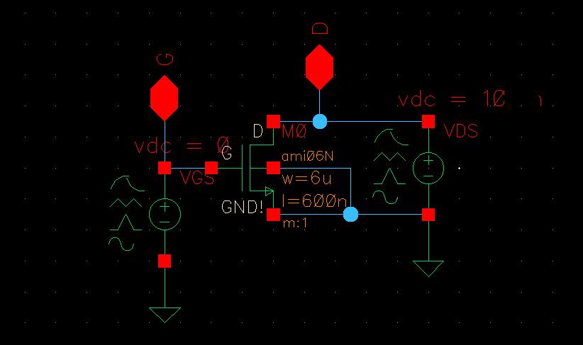
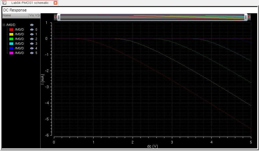
Part III: PMOS ID vs VSD
VSG varies from 0 to 5 V in 1 V steps and VSD varies from 0 to 5 V in 1 mV steps.
The simulation shows ID vs VSD at different values of VSG.
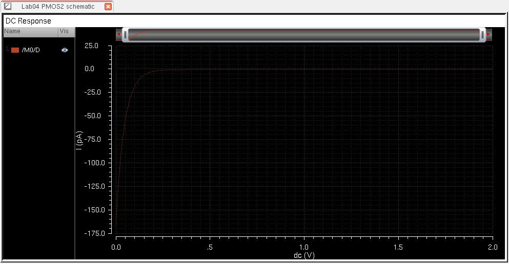
Part IV: PMOS ID vs VSG
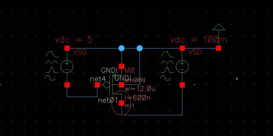
The simulation shows ID vs VSG when VSD = 100mV and VSG varies from 0 to 2V.
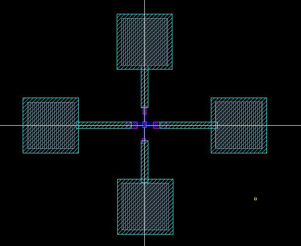
Part V: Layout of an NMOS transistor
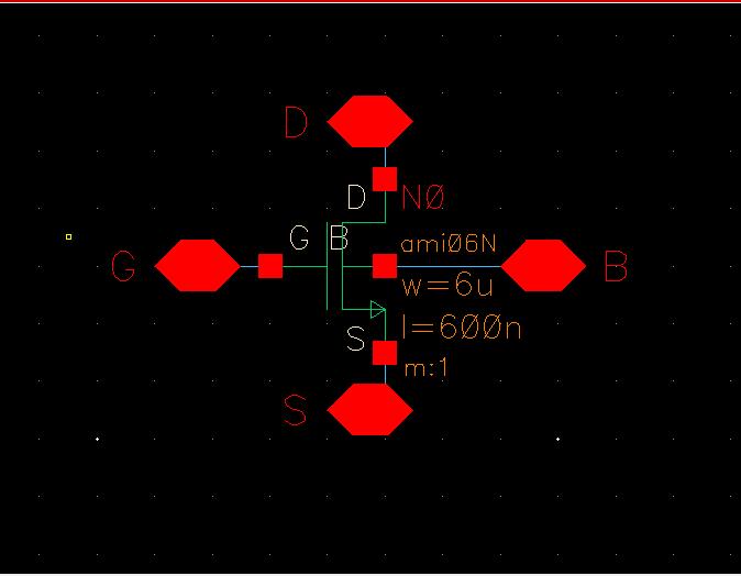
An NMOS layout requires a Ptap instance to connect the P-substrate Body to ground through metal1, and a m1_poly instance to connect the poly Gate to metal1.
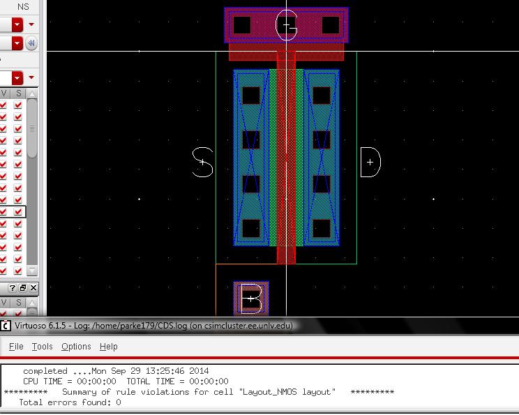
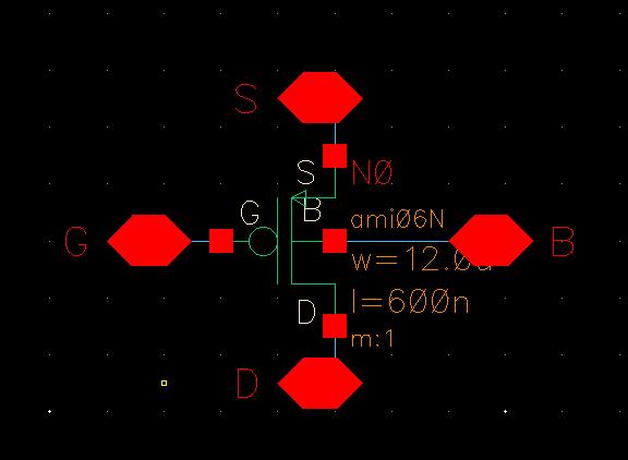
After laying out the NMOS, I made a simple NMOS schematic with pins to compare with an LVS.
I chose the 4-terminal version so that the layout and schematic can be used in any situation.
Before running an LVS, I added probe pads that will connect to each pin on the NMOS.
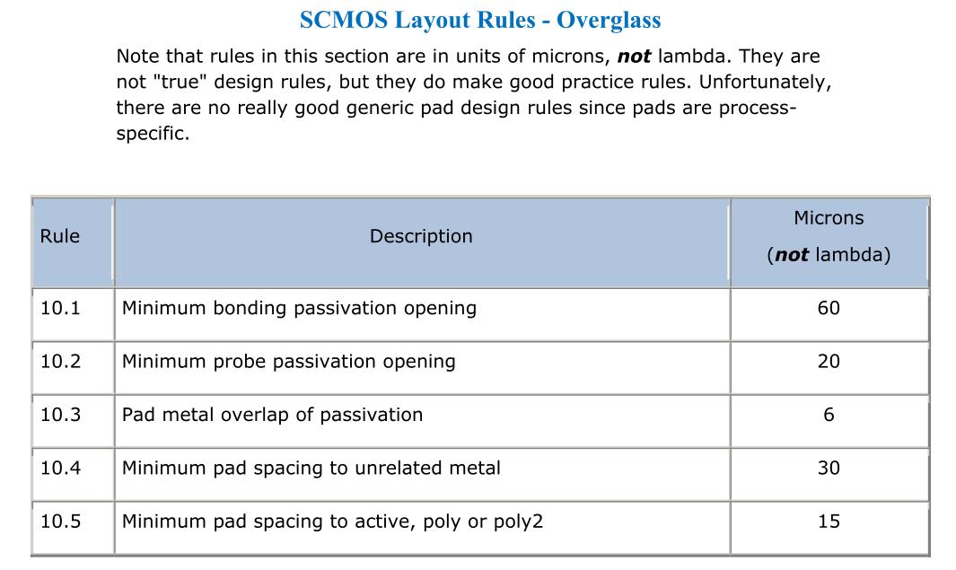
The required size of the pads can be found from the CMOS C5 process rules.
The via (and via2) connections must be 0.6X0.6 and be spaced apart by 0.9. Having multiple Vias improves the connection and maximum current that can flow through a wire.
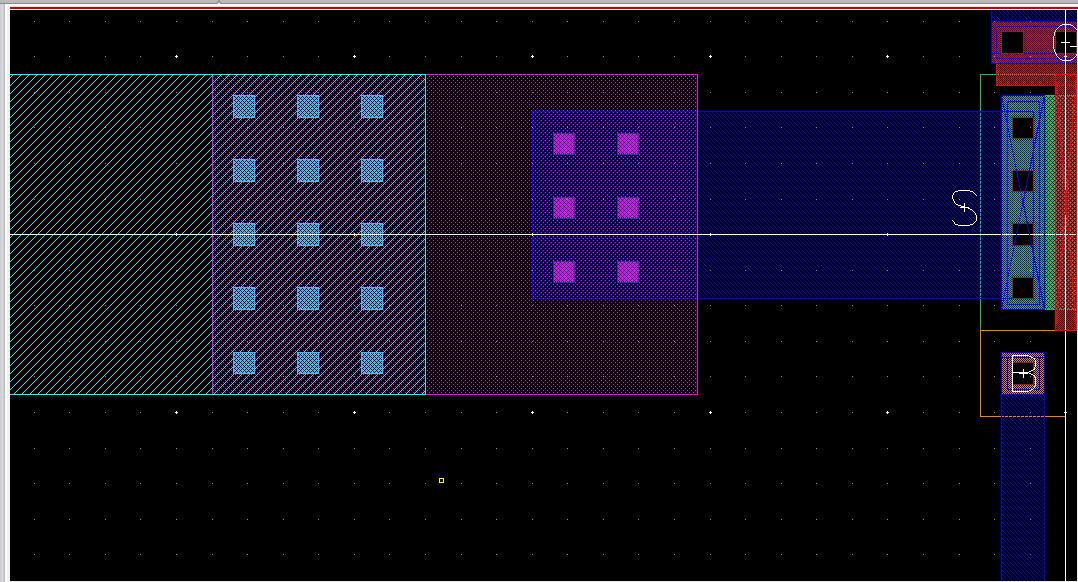
After adding each metal/via rectangle, it is a good idea to do a DRC test because there is likely to be a spacing or edge placement error.
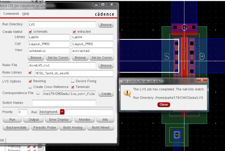
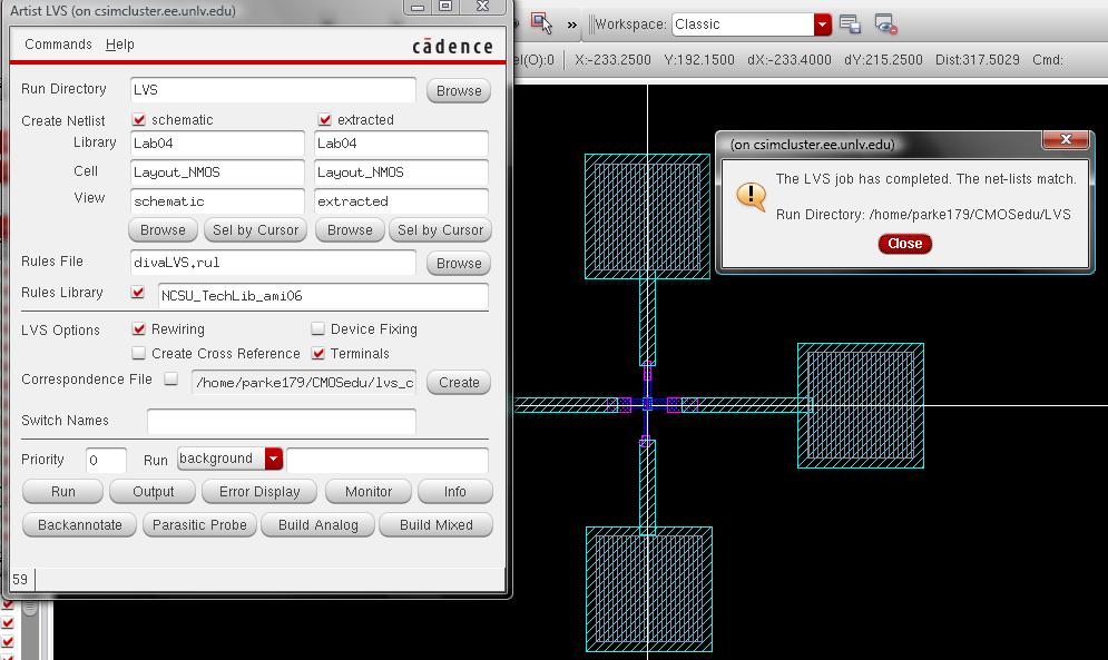
Once the layout is complete, the last step is to extract the layout and run an LVS.
Part VI: Layout of an PMOS transistor
Laying out a PMOS after the NMOS can be done quickly by copying the NMOS cellview and modifying it.
There are only a few changes to make:
1. Change the Ptap to an Ntap, since PMOS has a N-well body and not a P-well (P-substrate in the C5 process).
2. Replace the NMOS with a PMOS and Increase the Width of the PMOS to 12u. Reposition objects to make them fit.
3. In the schematic, change the NMOS to a PMOS and swap around the S and D pins.
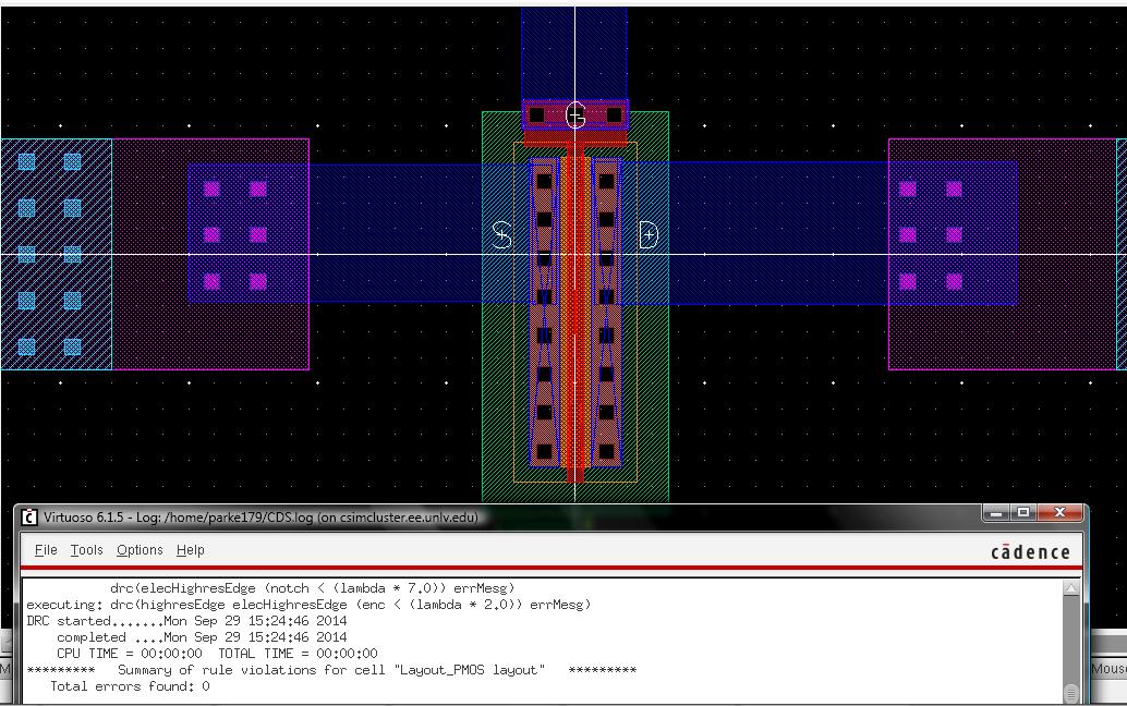
Perform a DRC then try an LVS. The LVS failed the first time, but was solved by replacing the old wires in the schematic to the pins.