Lab 03 - EE 421L
Authored
by Matthew Parker
parke179@unlv.nevada.edu
September 28th, 2014
Lab
description: The purpose of this lab is to layout a 10k N-well
resistor, then use that to layout a 10-bit DAC using the design from
lab 2.
The library for this Lab03 can be downloaded from the zip file located in this directory
http://cmosedu.com/jbaker/courses/ee421L/f14/students/parke179/Lab03/other/
Direct download link
Part I: Laying out an N-Well resistor
An
N-well resitor in the C5 process has a sheet resistance of about 800
ohms/square, and a minimum width of 12 lambda (3.6 um since lambda is
300 nm).
To make a 10k resistor, the N-well would need to be 10k/800 = 12.5 squares long.
A 12.5 square N-well at minimum width would have a size of 45 um X 3.6 um.
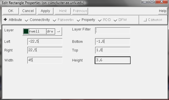
After
laying out the N-well resistor with metal 1 connectors, adding a
res_id, and extracting it, I noticed that the resistance was lower than
it should be.
The
reason the resistance is so low is because the metal-1 to N-well
connectors reduce the effective length of the resistor by about 2
squares.
To compensate for the connectors, I increased the number of squares to 15 and changed the dimensions to 50um X 3.6 um.
However,
50um/300nm = 83.333 lambda, which is not allowed by the DRC, so I
reduced it to the final dimensions of 49.8um X 3.6um.
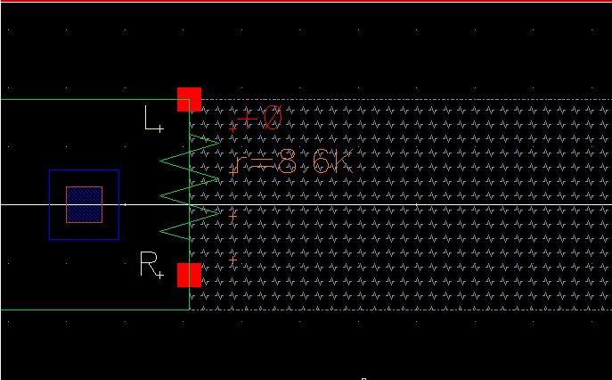
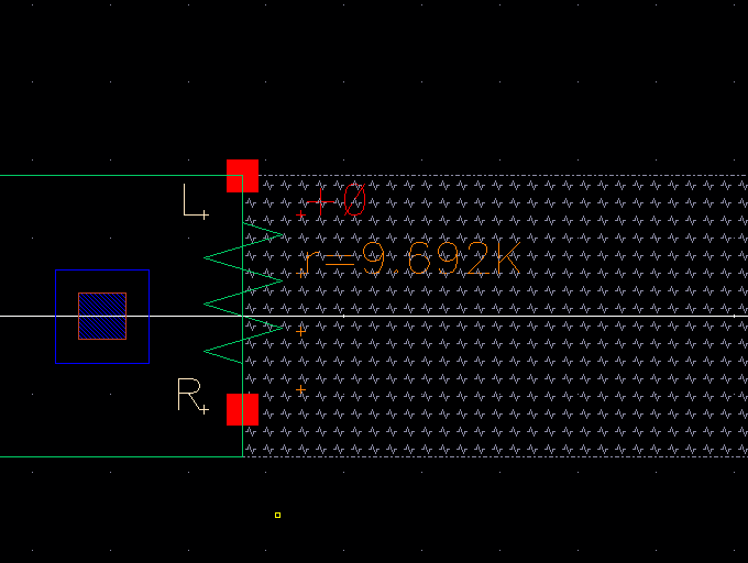
The total resistance at these dimensions should be (49.8/3.6 squares - 2 squares)* 800 ohms/square = 10,352 ohms.
The final exported value shows something a little less than this ammount, but it is close enough (about 3% off).
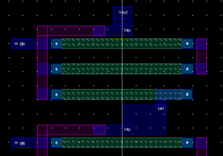
Part II: Laying out the Digital to Analog Converter (1-bit)
The
design for the DAC is the same as that used in lab 2. The 10-bit DAC is
made up of 10 1-bit DACs, and each 1-bit DAC is a simple R2R circuit.
The first step is to layout the resistors with minimum spacing, and adding metal1 rectangles that lead to the pins for in, top, and bot.
A DRC check at this point should show no errors.
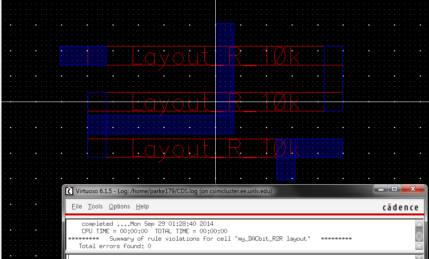
The next step is to create pins, then export the layout and do a Layout Vs Schematic (LVS) check.
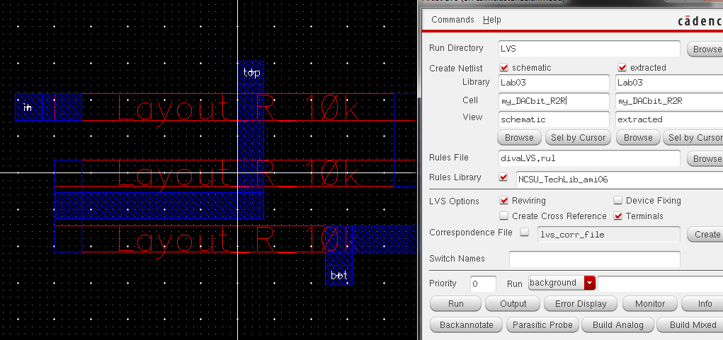
At
this point, I got an error saying that the netlists do not match. After
examing the extracted layout file, it became clear that the metal1
connections between the resistors were not behaving correctly. For some
reason, they would count as seperate nets (for example, N4 and N5).
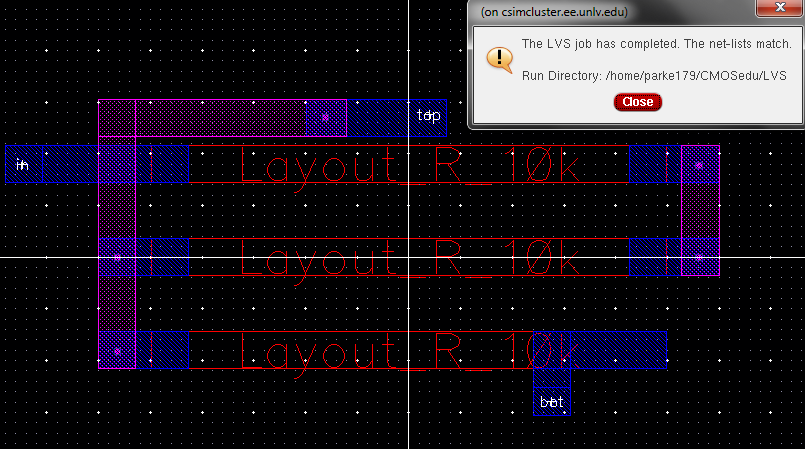
To fix this problem, I remade the connections and routed them through metal2 using a via rectangle.
(Side note: I was unable to make a via any larger than exactly 0.6x0.6 without getting a DRC error).
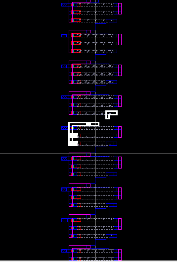
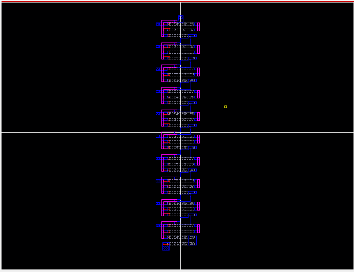
Part III: Laying out the Digital to Analog Converter (10-bit)
After making the 1-bit DAC (R2R) layout, the final step is to make a 10-bit DAC.
In order to actually see the contents of each R2R, the display "stop" setting was set to 20.
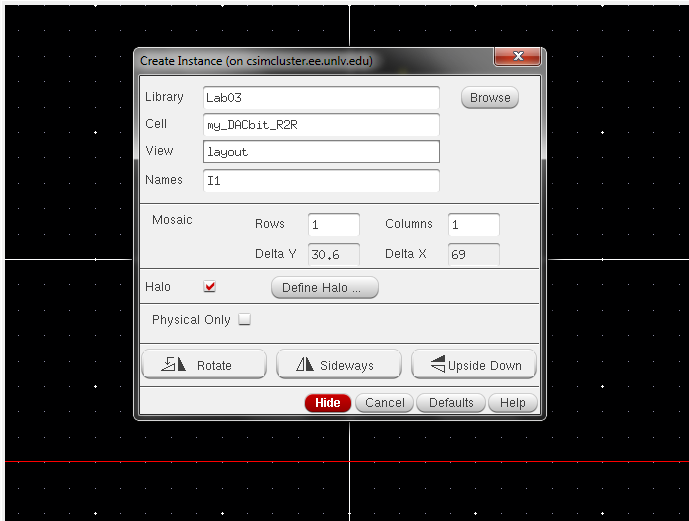
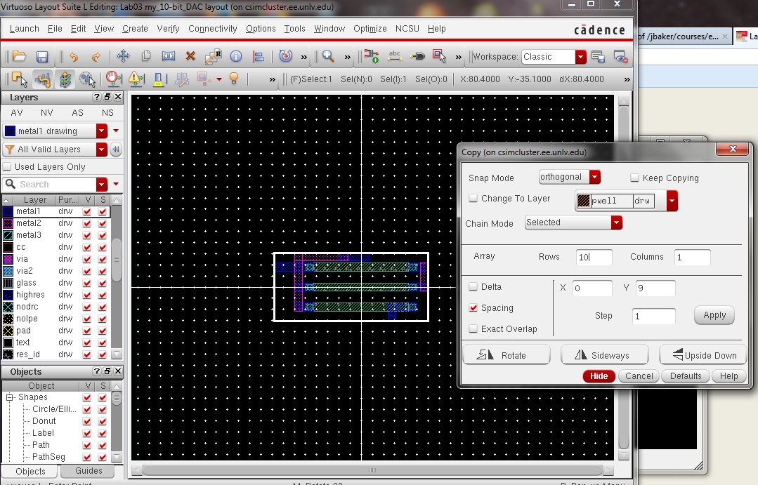
To
quickly make 10 of the R2R with even spacing, I used the copy command
and set the number of rows to 10 and spacing to 9 (later changed to 4.5
for even tighter spacing) then hit apply.
After a DRC test to verify the spacing was okay, I added metal1 connections from every bot to every top that should be connected, then did a DRC test.
After the DRC test succeeded, I added all the pins, making sure to name ground gnd! and set each B[0..9] to be an input.
After
doing a LVS with the pins added and the layout extracted, I was
suprised to see the test fail. After looking at the exported layout, I
saw a simple mistake; I forgot one of the metal1 connections.
After the easy fix of adding the metal1 rectangle, the LVS succeeded.
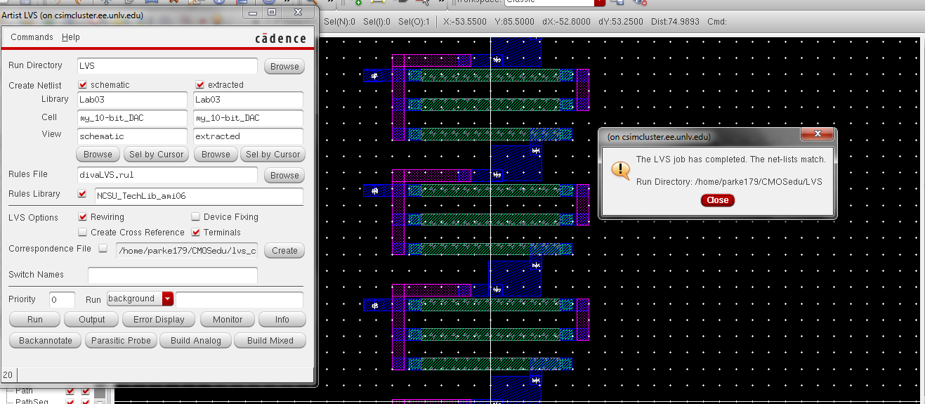
Figure 12: View of the entire layout (in the export)
The library for this Lab03 can be downloaded from the zip file located in this directory
http://cmosedu.com/jbaker/courses/ee421L/f14/students/parke179/Lab03/other/
Direct download link