Lab 02 - EE 421L
parke179@unlv.nevada.edu
Part I: Examining the Ideal ADC-DAC Circuit
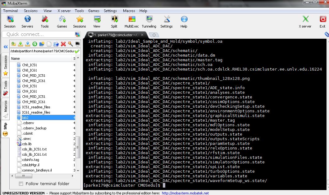
Step 1: Download lab2.zip and extract it to the CMOSedu directory. Then add this line to the cds.lib file.
DEFINE lab2 $HOME/CMOSedu/lab2
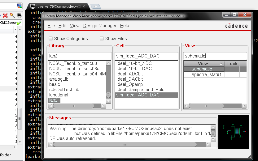
Step 2: Open Virtuoso and open the ideal 10-bit ADC schematic found in lab2 (sim_Ideal_ADC_DAC).
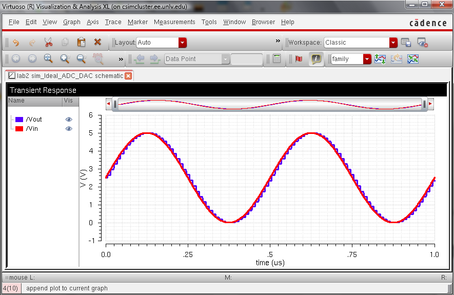
Step 3: Load the simulation and verify that it matches the example provided.
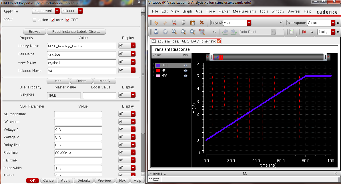
Step 4: To determine which bit in the ADC is the least significant bit, and to understand what the binary value represents, I changed Vin to be a linear pulse from 0 to 5V and looked at bit1 and bit9. From the simulation, it is clear that bit0 is the LSB. The data encoded in binary should split 5 volt range into 1024 levels, which comes out to 4.88 mV (about 5 mV).
Part II: Changing the 10-bit DAC
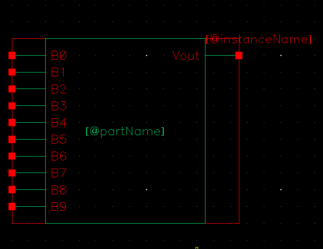
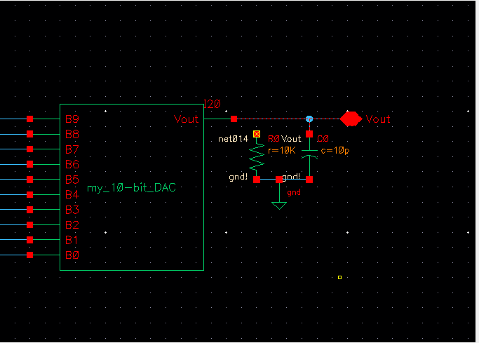
Step 1: In the file manager, make a copy of the ideal 10-bit DAC, Then create a new schematic by going to File->new->cell view and selecting Schematic from the drop-down menu.
Step 2: In the schematic, create 3 resistors and add pins for input, top, and bottom.
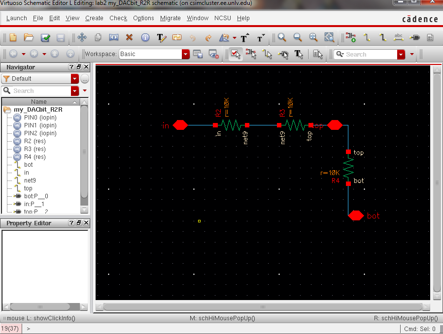
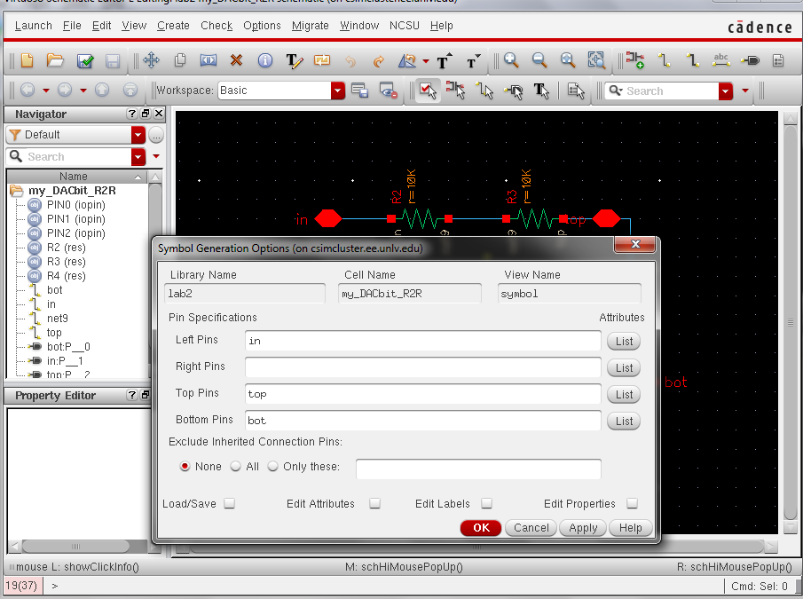
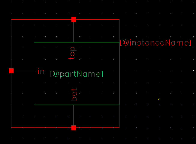
Step 3: Creat a symbol by going to Create->Cell View->From Cell View. Adjust the locations of pins on the second menu after hitting ok.
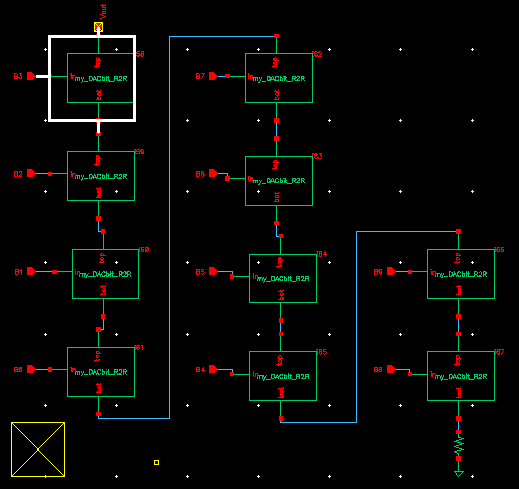
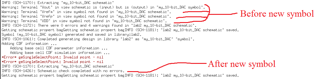
Step 4: Go into the copy of the 10-bit DAC and replace all the 1bit DACs with the R2R version that was just created. Add an extra restior to the bottom of the last one. After the schematic is done, the Save and Check will give 4 warnings about the unused pins that were deleted, sich as Vrefm. After making a new symbol, these warnings will go away.
Figure 08 - Updated DAC schematic
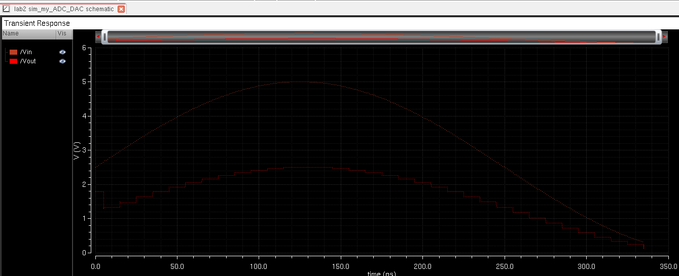
Step 5: Now the new DAC should behave the same way as the ideal DAC, so put it into a copy of the ADC-DAC sim schematic and simulate it.
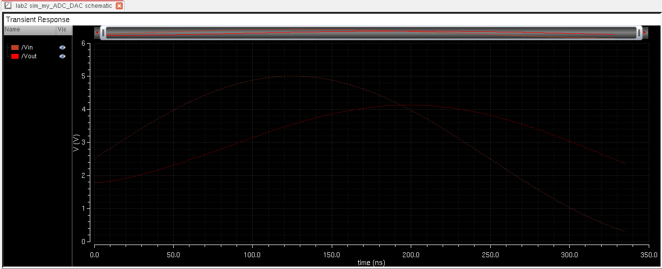
Figure 13: ADC-DAC circuit with the new DAC
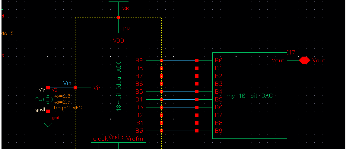
Figure 12: (Bad) Simulation after changing DAC
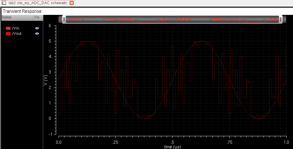
The simulation in figure 12 shows that the DAC is not a perfect substitute (I made a mistake somewhere). The mistake I made was that the pins were not labeled correctly. I had B0 going to B9 and so on. Figure 13 is the correct simulation results.
Figure 13: (Good) Simulation after changing DAC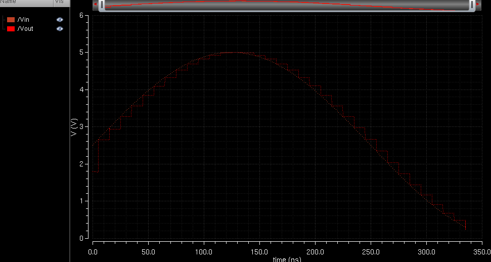
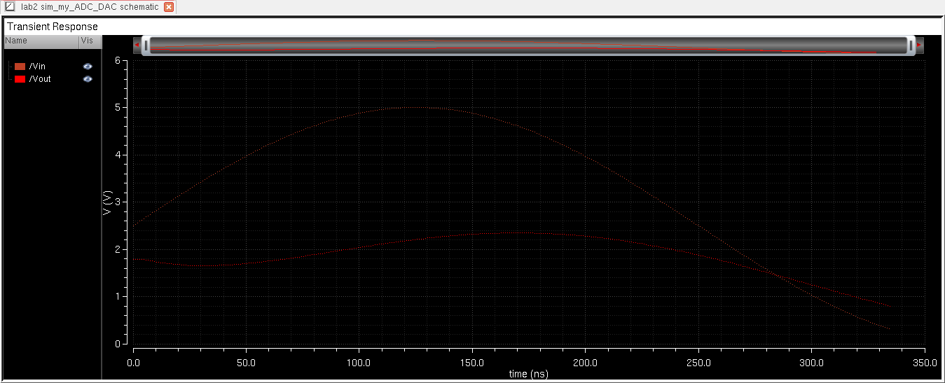
Step 6: Run simulations with a load capacitor and resistor.
With just a resistor: The magnitude of the output decreases. When Rload is 10k, the magnitude is halved.
With just a capacitor: The phase of the output is delayed, but the output is smoother. The delay is equal to about 0.7RC.
With both: Both effects are combined, so the output is smoothed, phase delayed, and reduced in magnitude.
Step 7: Find the output voltage of the DAC.
Figure 18: the DAC circuit as R2R repeated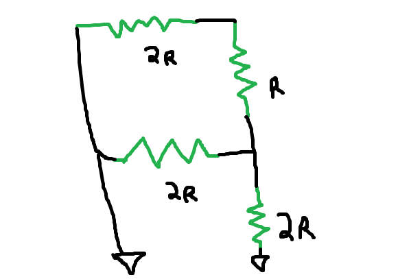
From figure 18, it is easy to see that the bottom two resistors are in parallel. 2R//2R = R.
After that, the R is in series with another R. R + R = 2R.
Then the process repeats for each bit in the DAC, making the final output voltage equal to R (10K ohms)
Step 8: Find the delay with a capacitor attached to Vout and a pulse at B9.
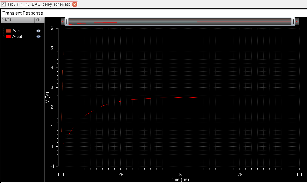
The delay is expected to be 0.7RC = 0.7*10k*10p = 70ns.
In the simulation, the time it takes for Vout to become half of the maximum (1.25V, 2.5V) is about 75ns (0.075us).
Step 9: Discuss what happens if the resistance of the switches isn't small compared to R.
The output voltage will be reduced because the switches will steal power away from the DAC.