Project - EE 421L
Authored
by Christopher Mikhael,
Email: Mikhaelc@unlv.nevada.edu
11/24/2014
Project Part 1:
Objective:
The
objective of this part of the lab is to create a working 8 bit ALU. In
order to do this I first created a 1 bit ALU using components used in
the previous labs.
After the labs were created the ALU was then
simulated to make sure that it is working correctly. The ALU has the
functions: AND, OR, A+B, and A-B.
1-bit ALU
The following schematics were created to make the ALU.
| Schematic | Symbol |
| INVERTER | 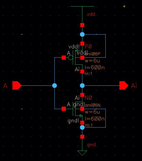 | 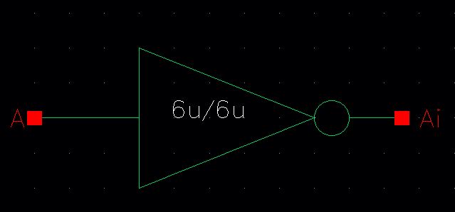 |
| OR | 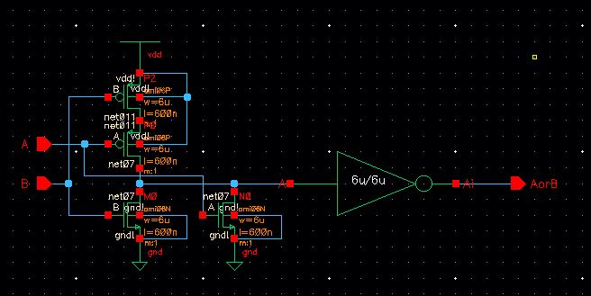 | 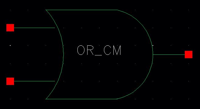 |
| AND | 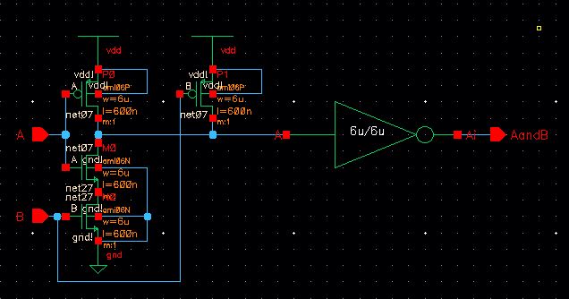 | 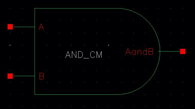 |
| MUX | 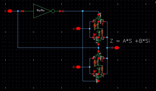 | 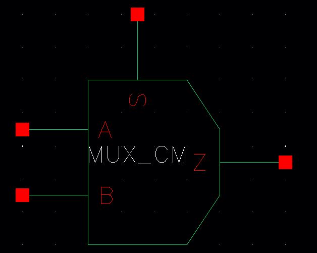 |
| FULLADDER | 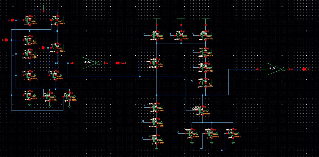 | 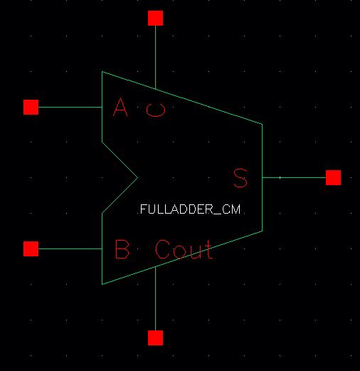 |
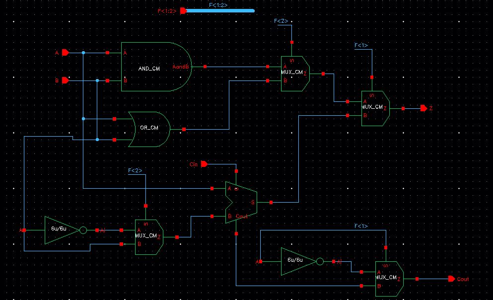
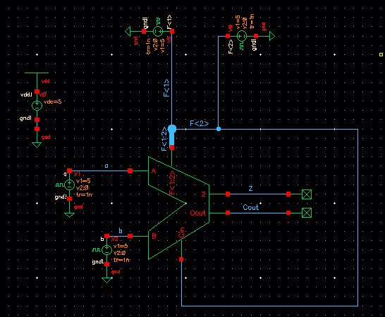
We then put the components together to make the onebit input output ALU
This
is shown in the schematic below. Notice that the MUX acts as a switch
choosing the logic type. The logic for the F input of the MUX are as
follows:
| F<1> | F<2> |
| ADD | 0 | 0 |
| SUB | 0 | 1 |
| OR | 1 | 0 |
| AND | 1 | 1 |
Schematic:
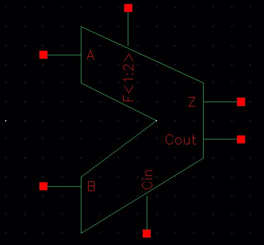
Symbol
Then simulate the output showing all possible outputs for the ALU.
Order of Outputs in Simulation Below
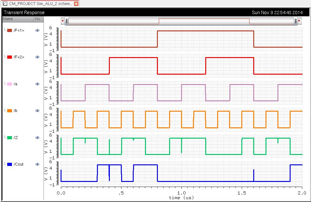
As
we can see when F<1> and F<2> equal 0 the simulation shows
that A and B are adding. When F<1>=0 and F<2>=1 subtraction
occurs. Subtraction works by first inverting B. The inverted form of B
is then added by one. Then A nad B are added together to produce the
correct subtraction. The COUT pin acts as a negative sign when 0 and a
positive sign when 1. When F<1>=1 and F<2>=0 the bits will
OR each other producing a result of 1 whenever A or B is equal to 1. An
extra multiplexer was added to the COUT pin to differentiate when the
COUT pin should be active. During AND and OR operation COUT is set to
0. Then the AND gate is when F<1> and F<2> are both set to
1. The output should be 1 only when both A and B are 1.
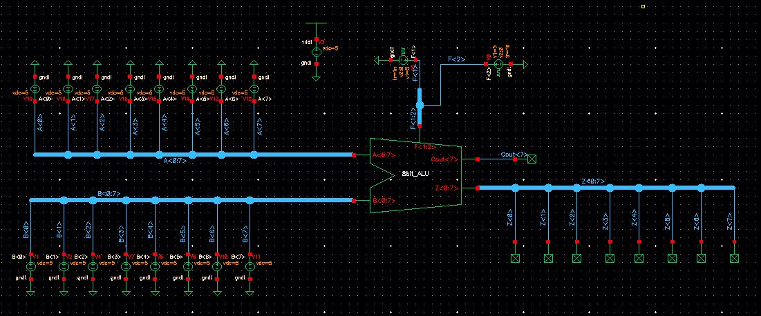
8bit ALU
To create the 8 Bit ALU, the 1 bit is used with busses to show the 8 schematics. This is shown below:
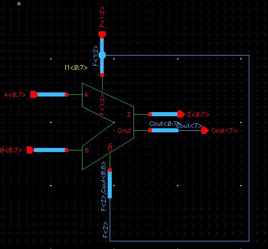
To
create the 8 bit ALU we have to take the COUT of the first ALU and send
it to the CIN of the next. Since subtraction takes place when
F<2>=1 and subtraction needs a Cin of 1 we make the first bit in
CIN eqaul to F2 as shown above.
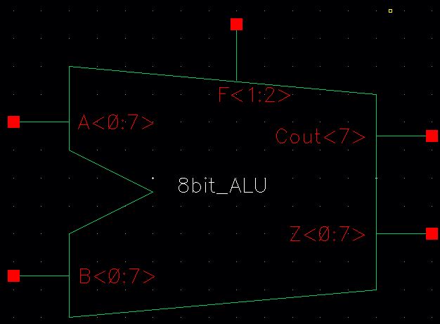
Symbol:
Simulation Schematic
Notice
for this schematic we will be inputing A=11111111 and B =
11111111 into the ALU. We should see the following result for each
operation:
ADD: 111111110
SUB: 100000000
OR: 011111111
AND: 011111111
***The first bit is COUT
The simulation is shown below:
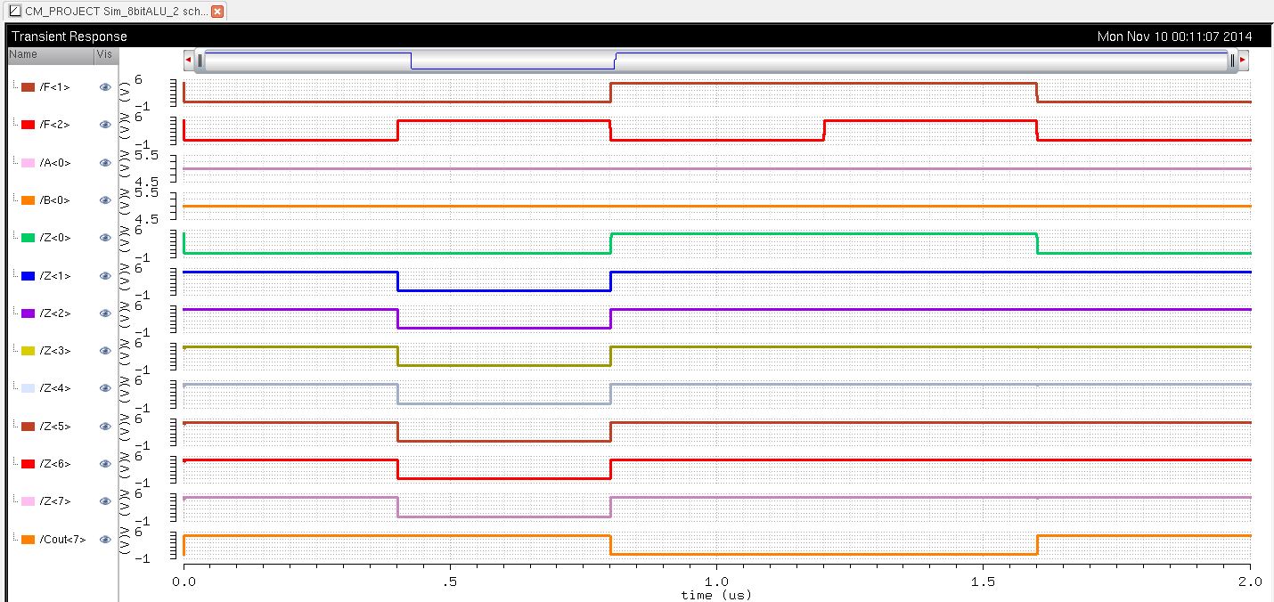
The results are shown below in the simulation. A<0> and
B<0> are the only values shown in the simulation to keep the
window size managable but all other outputs in A and B are set to 1 for
this simulation.
Project Part 2
For
this part of the project we will be creating the layout for the 8-bit
ALU. To do this we first must create the 1-bit ALU, this will be later
cascaded 8 times to create the 8-bit ALU.
To create the 8-bit ALU we will have to layout the AND, OR,
FullAdder, Multiplexer, and inverter. Although some of these components
were done in previous labs, some were motified to
have the same footprint so that GND and VDD align in the layout.
Each component and its layout are shown below:
| Layouts |
| Inverter | 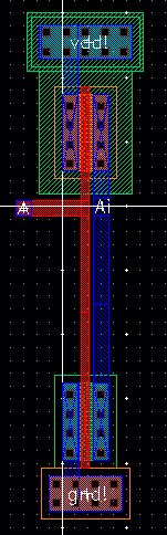 |
| AND | 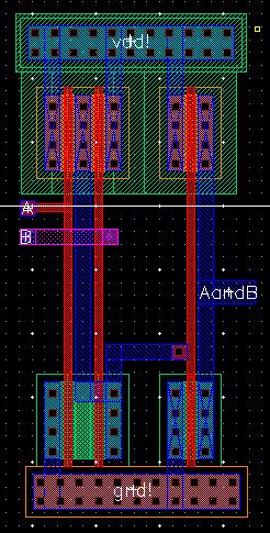 |
| OR | 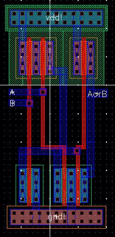 |
| FULL ADDER | 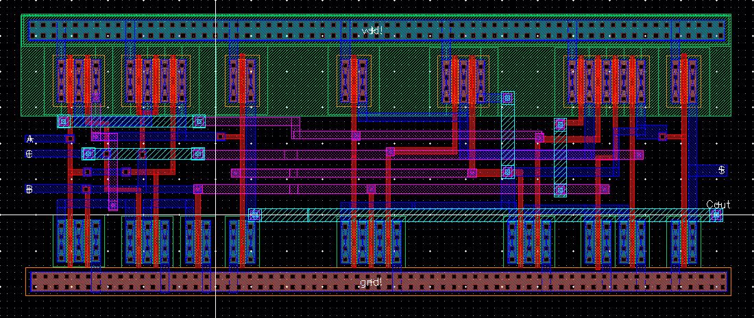 |
| MULTIPLEXER | 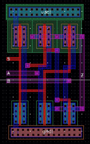 |
After
each of the above layouts are completed and LVS properly we can now
create our 1-bit ALU. This is shown in the layout below:
Above we have an the following gate in the following order: OR, AND, Inverter, Mux, Mux, Adder, Mux, Inverter, Mux
After the schematic is complete be sure to LVS the schematic:
We
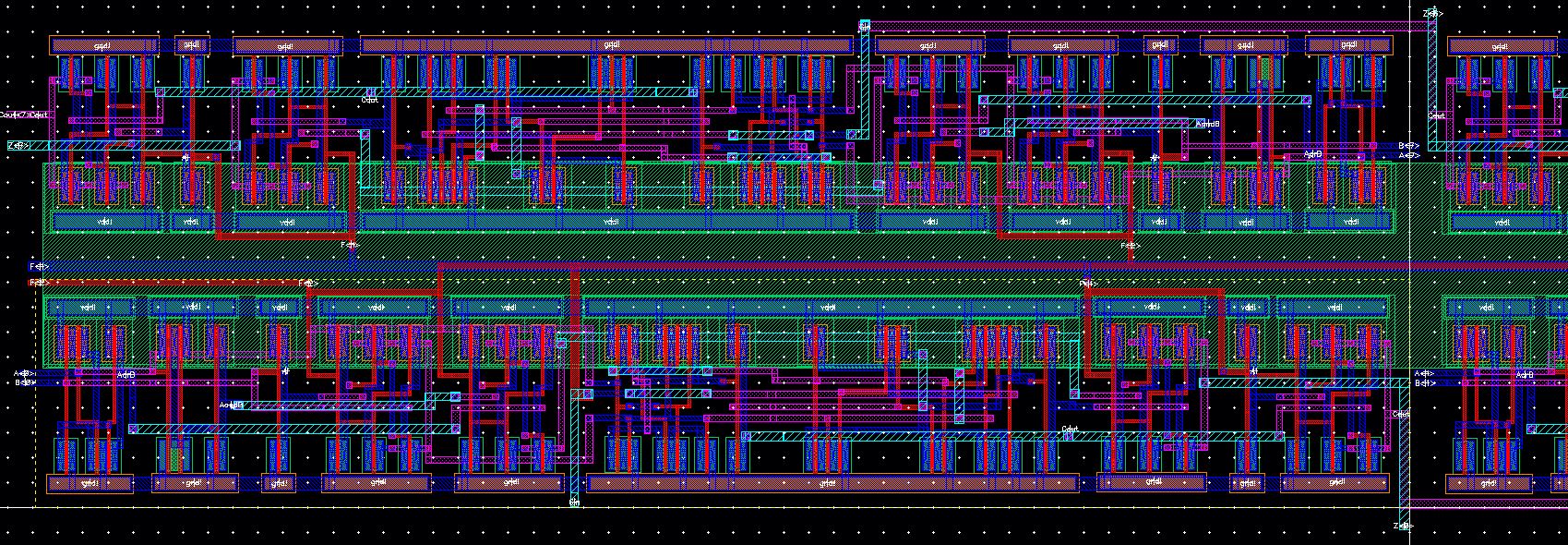
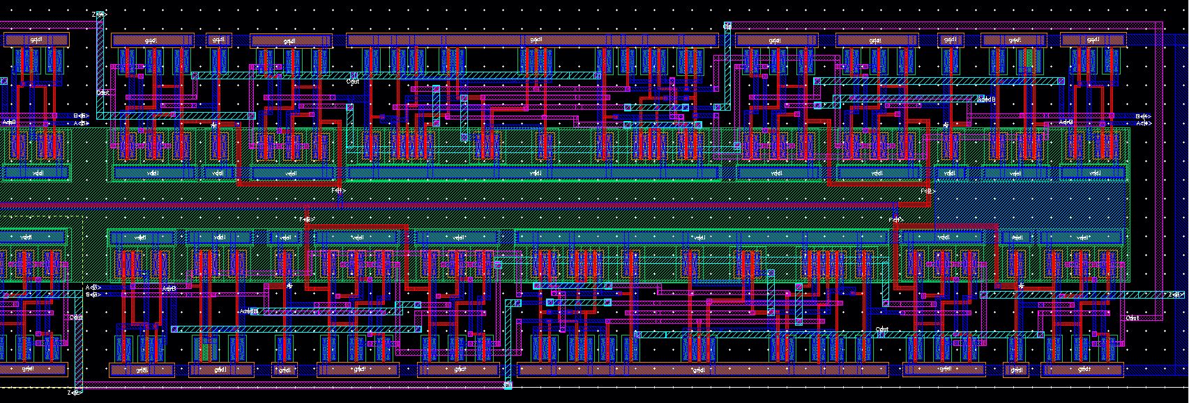
then use the 1 bit instance and cascade it 7 times to produce 8 ALUs.
We then connect the F2 and F1 connections together and label them
appropriately. We also have to make sure the first Cin bit is sent the
F2 signal. Then the cout of each bit is then sent to the Cin of the
next bit, until it gets to the last Cout. Also be sure to label each
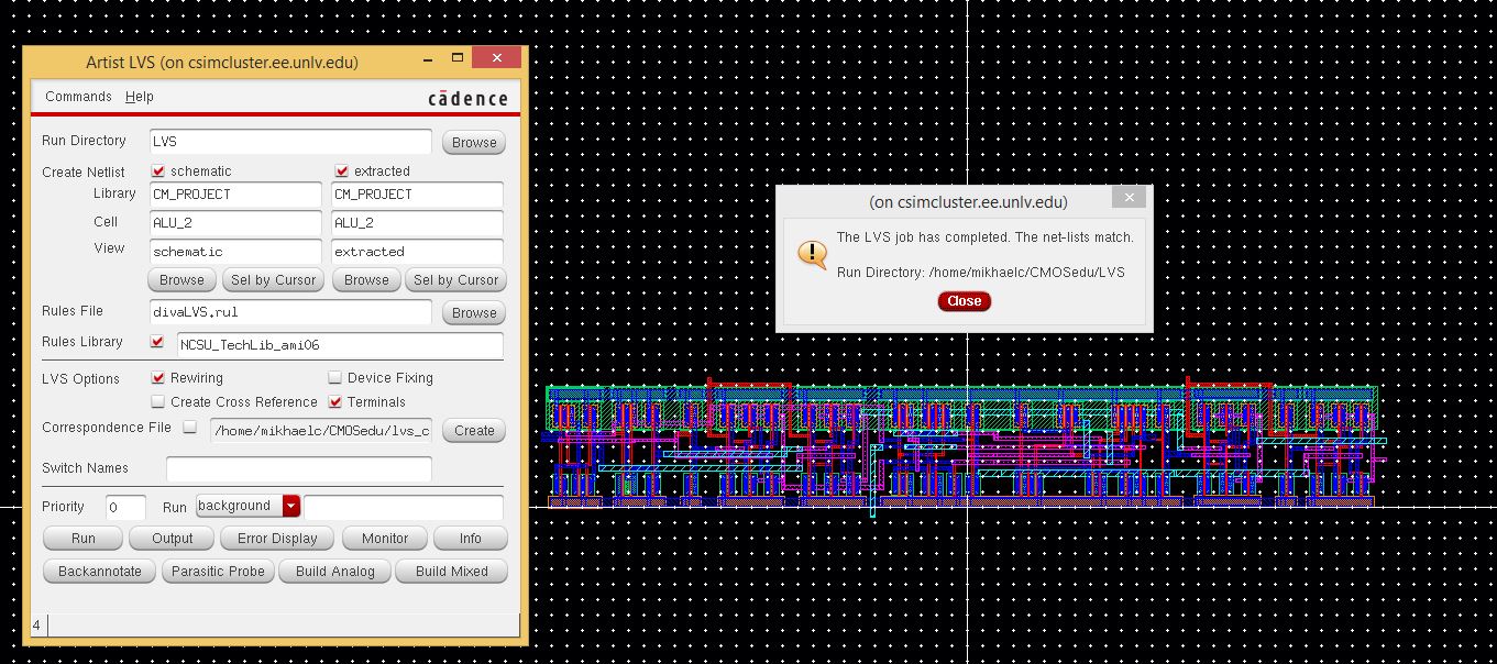
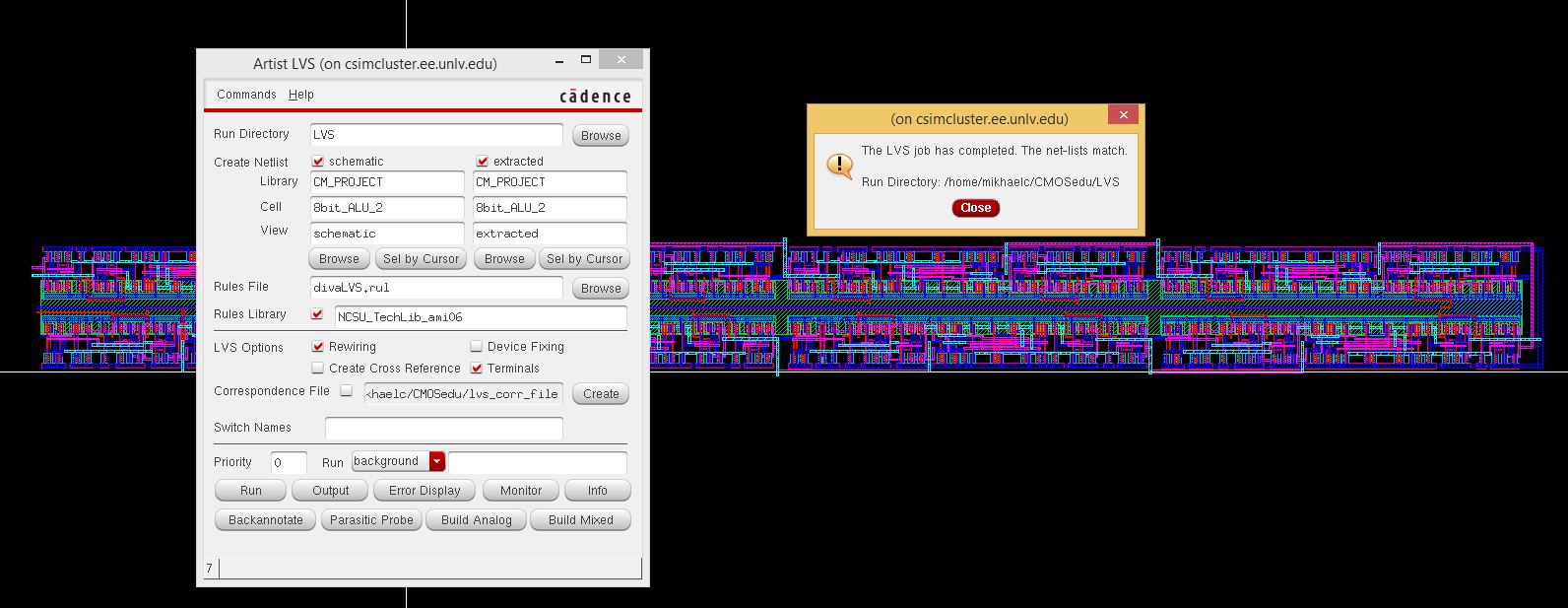
pins connected to the bus. After this is complete DRC, Extract and LVS
the layout. The layout is shown below as well as the LVS check.
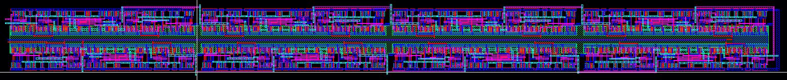
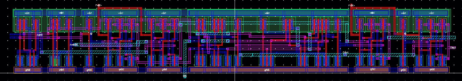
Front and End of ALU: Note the Bottom of the ALU is the beginning and the Back Top of the ALU has Z<7> and Cout
This is the other end of the 8bit ALU where the ALU wraps back around
The net-list match for the LVS
Proj directory: CM_PROJECT
In the directory all sims and schematics have "_2" to show the F2 with the bus. Example: ALU_2 and 8bitALU_2is the correct file.
BE SURE TO BACK UP ALL OF YOUR PROJ CONTENTS
(zip and email your work to yourself).