Lab 6 - EE 421L
Objective:
The objective of this lab is to become familar with the use of buses in order to use arrays for inputs. This is useful because it allows us to make test out multiple outputs easier and creates a simpler prcoess flow than duplicating components.
| NAME |
Schematic |
Symbol |
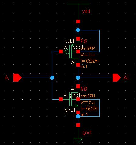
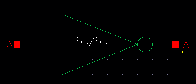
| Inverter |
|
|
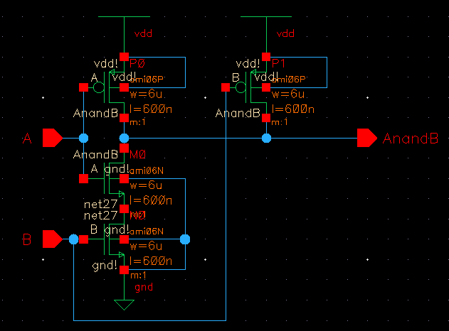
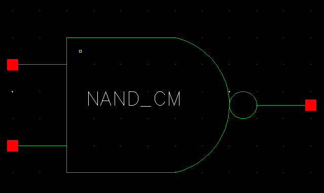
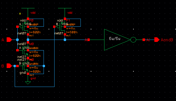
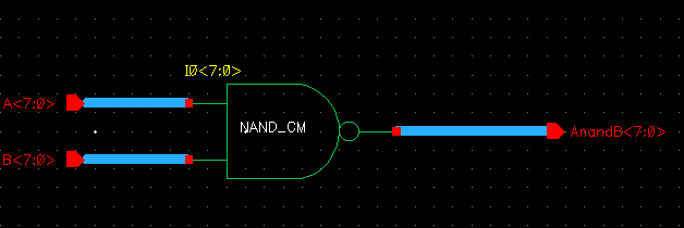
| NAND |
|
|
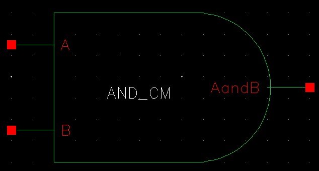
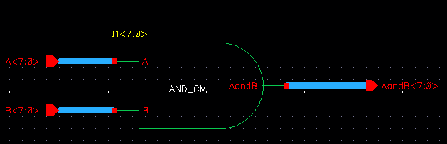
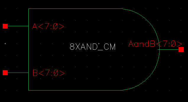
| AND |
|
|
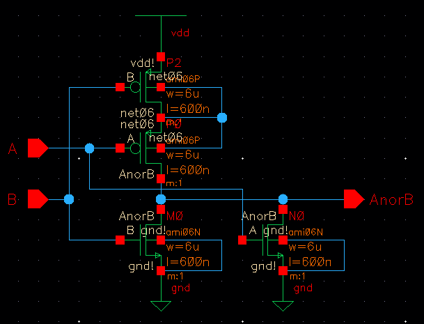
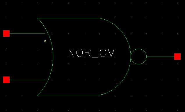
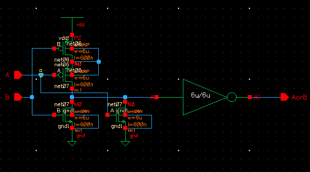
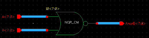
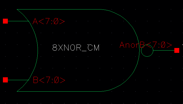
| NOR |
|
|
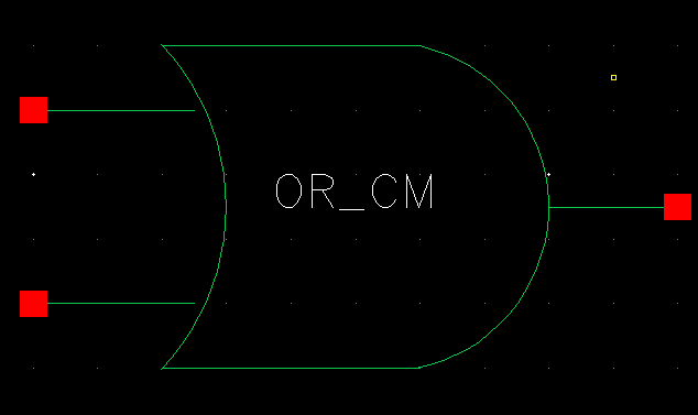
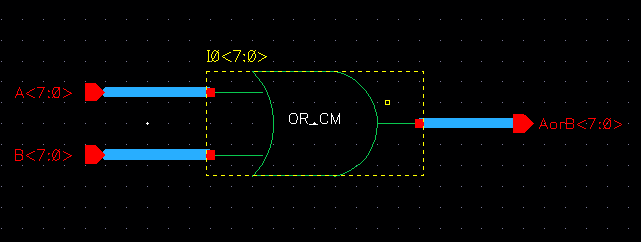
| OR |
|
|
We then took these instances and connected 8bit busses to the inputs and outputs of each termianl as shown below:
| NAME |
Schematic |
Symbol |
| Inverter |
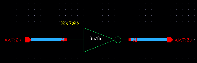 |
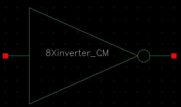 |
| NAND |
 |
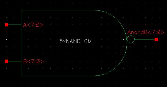 |
| AND |
 |
 |
| NOR |
 |
 |
| OR |
 |
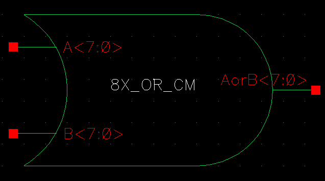 |
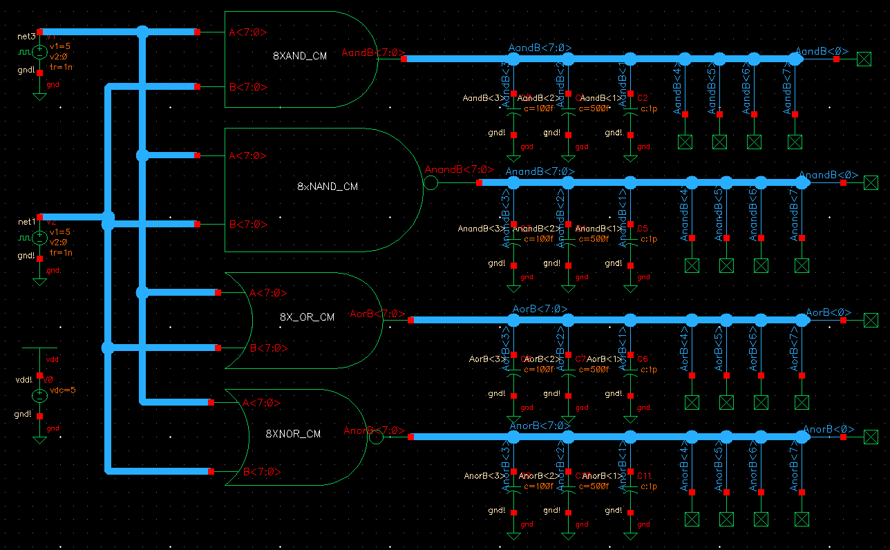
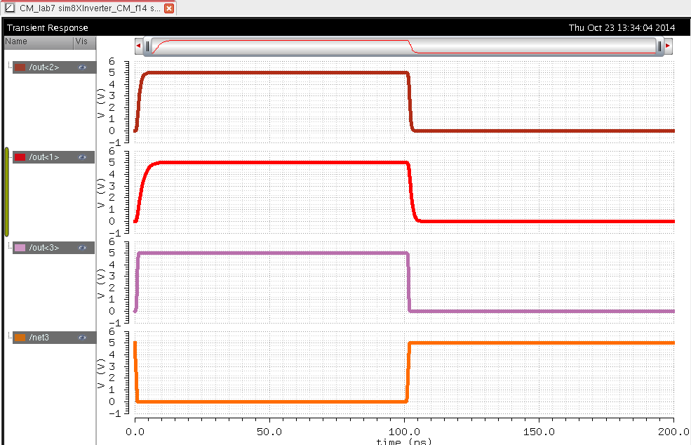
After the above schematics and symbols were created, they where simulated by placing 3 capacitors of different sizes onto seperate branches of the output bus. This is shown below. To perform this be sure to labe the bus as well as each branch created. Even though some of the branches aren't being used they still have to be labeled and connected to no connects for the schematic to pass DRC and sim correctly. The simulation schematics and Sims are shown below:
INVERTER Schematic
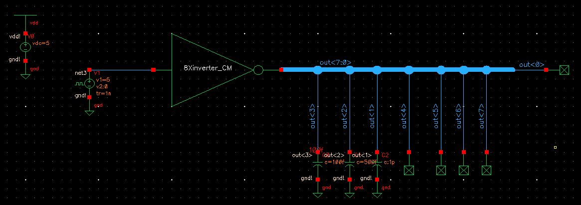
Simulations:
| NAME |
Simulation |
| Inverter |
 |
| AND |
 |
| NAND |
 |
| OR |
 |
| NOR |
 |
The
logic for this bit was still correct. As we can see from the
simulations when the capacitance is high we get a rounder output with a
larger delay. When the capacitance is shorter the shape of the the
output is more square like and has a smaller delay. This is very
important to know in order to understand how paracitic capacitance can
affect the circuit being used.
All the simulations above performed the correct logic for their respective gate. The only wierd effect was the NOR gate which operated correctly but had a voltage of about 1.5 volts when it should have been 0V when A=0 and B=1.
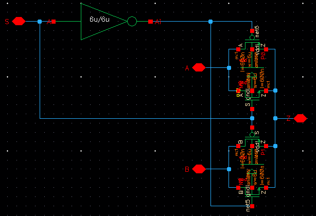
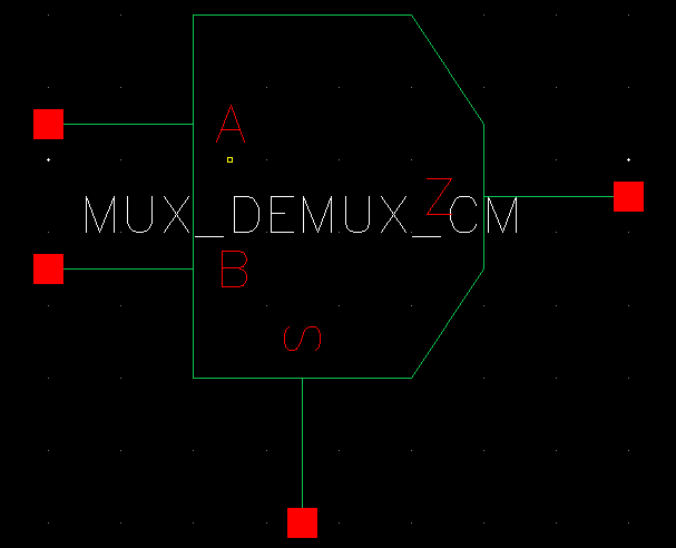
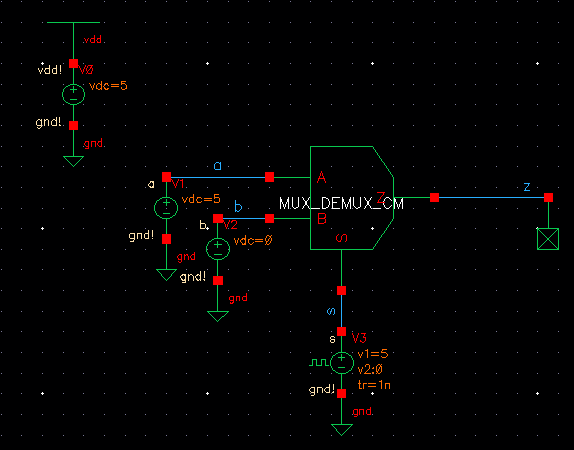
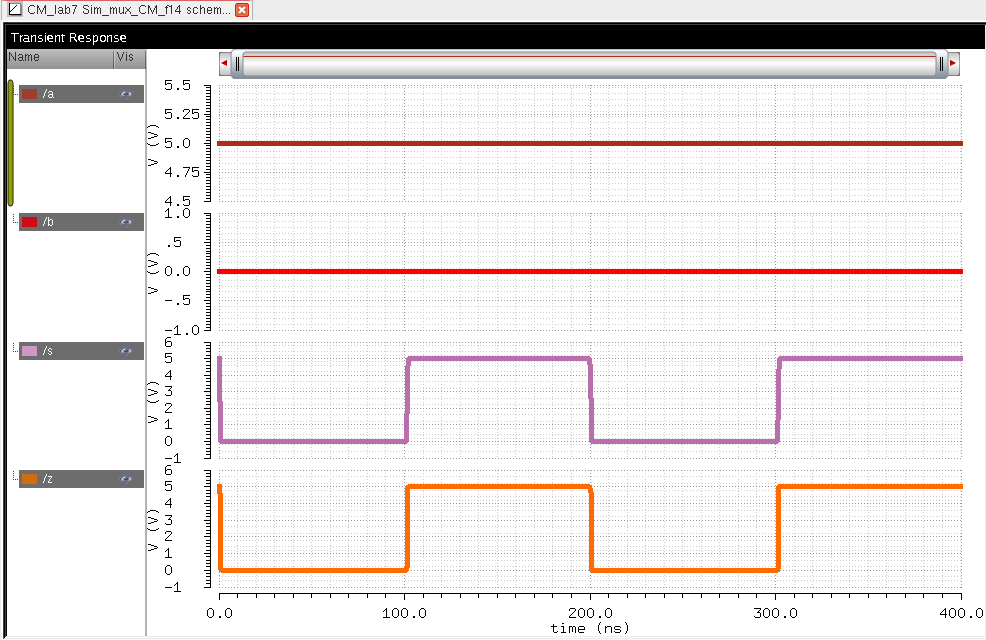
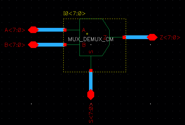
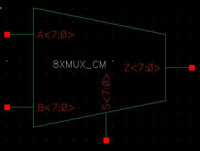
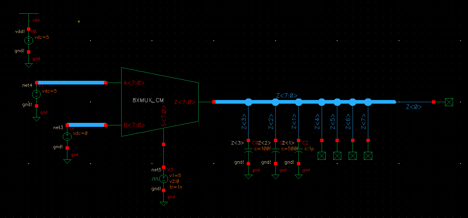
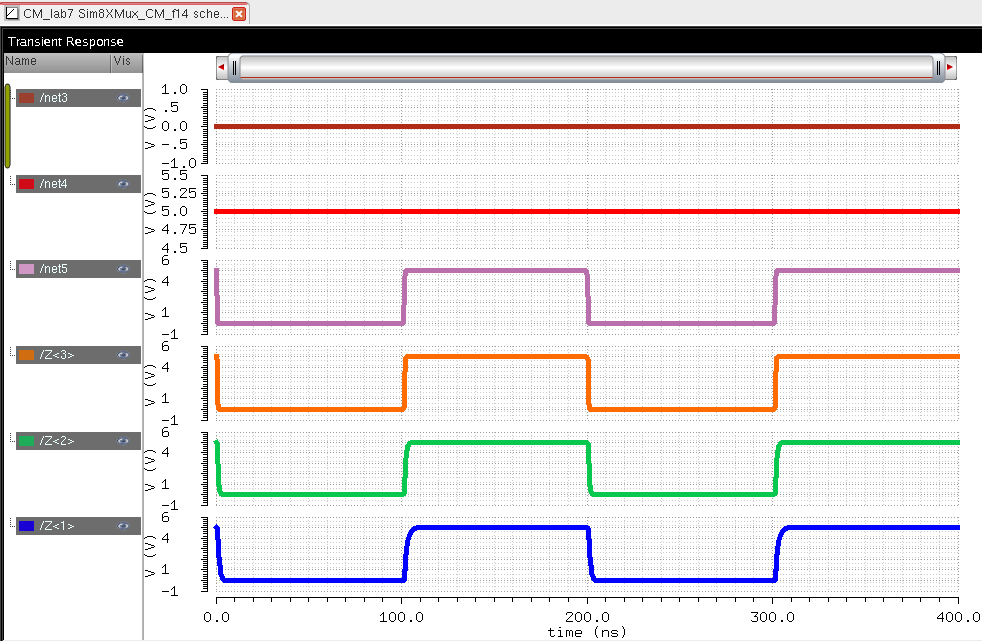
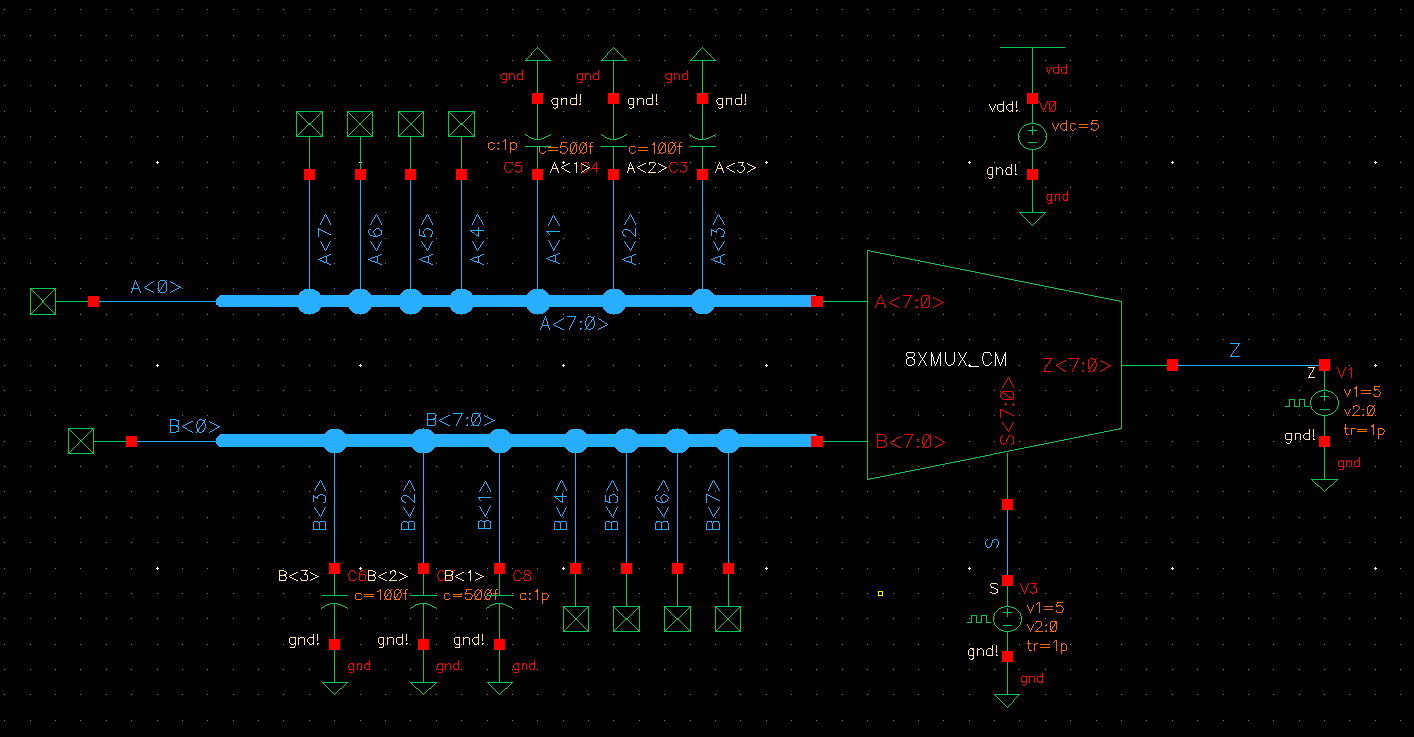
MUX/DEMUX
The next part of the lab was to create a MUX gate and a DEMUX using the same schematic. Then to perform the same with an 8 bit MUX/DEMUX. These are shown below:
| Simulation Schematic |
Simulation |
|
| MUX |
 |
 |
| DEMUX |
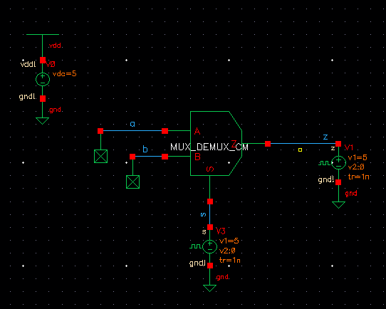 |
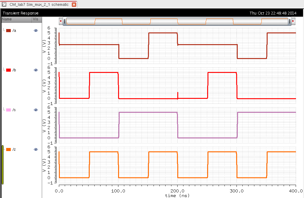 |
| Name |
Simulation Schematic |
Simulation |
| MUX |
 |
 |
| DEMUX |
 |
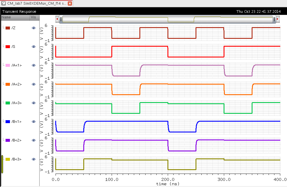 |
As seen above the 8 bit MUX/DEMUX works exactly the same except more inputs and outputs can be connected.
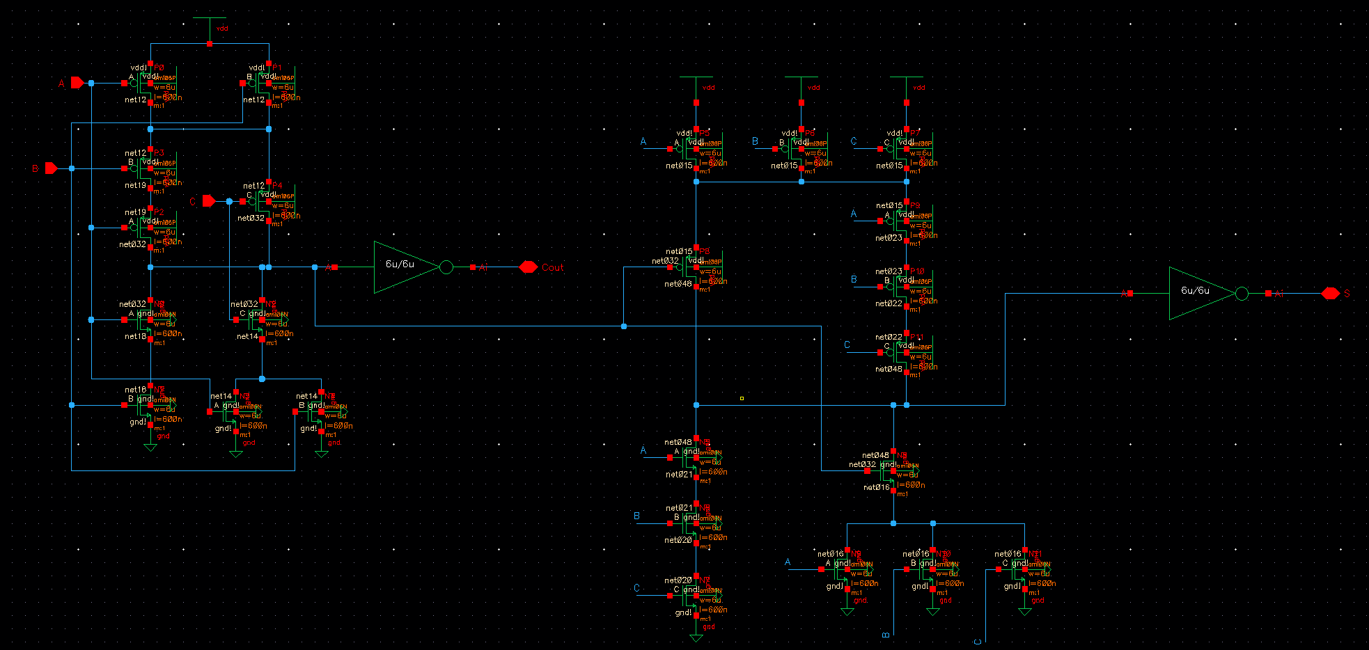
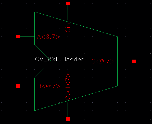
FULLADDER
Next we created the schematic and symbol for a full adder as well as the simulation and layout. The operation of a FULLADDER takes an input to A and B terminals as well as a C in bit. These bits are summed together. If the sum has more than one bit than the bit is carried, similar to normal addition. This is shown below:
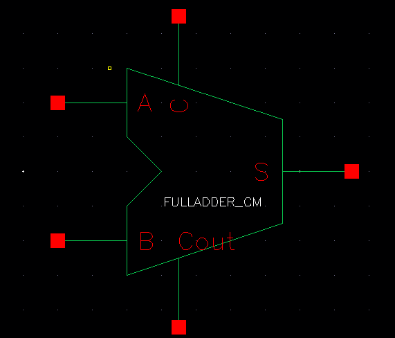
FULLADDER SYMBOL
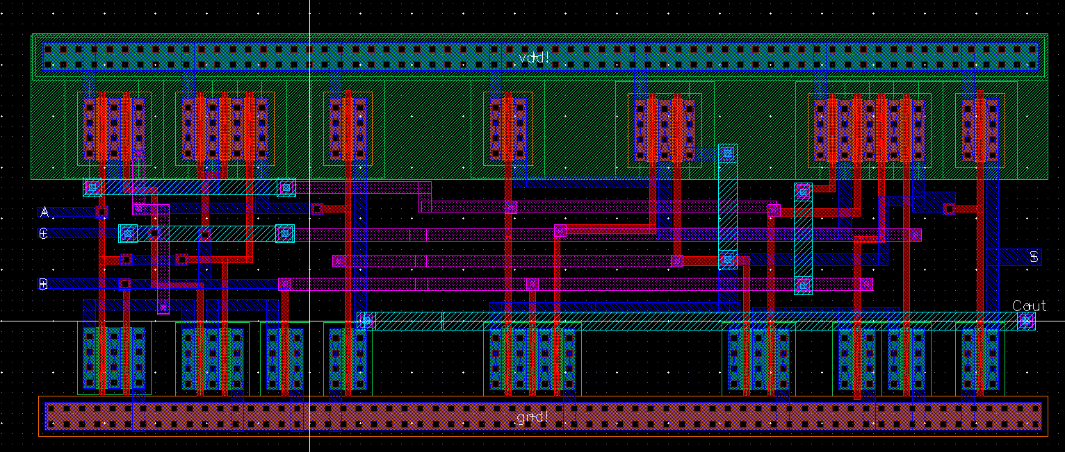
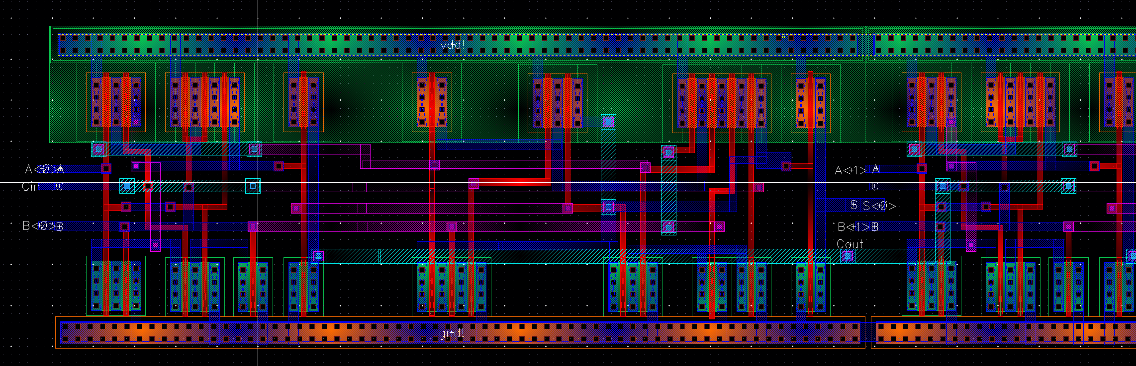
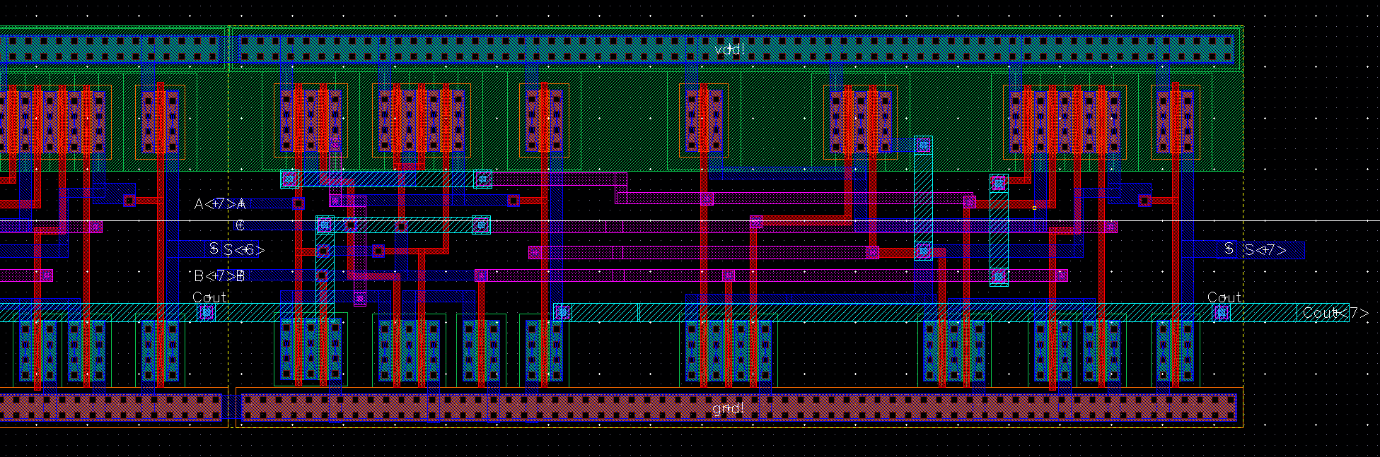
Full Adder Layout
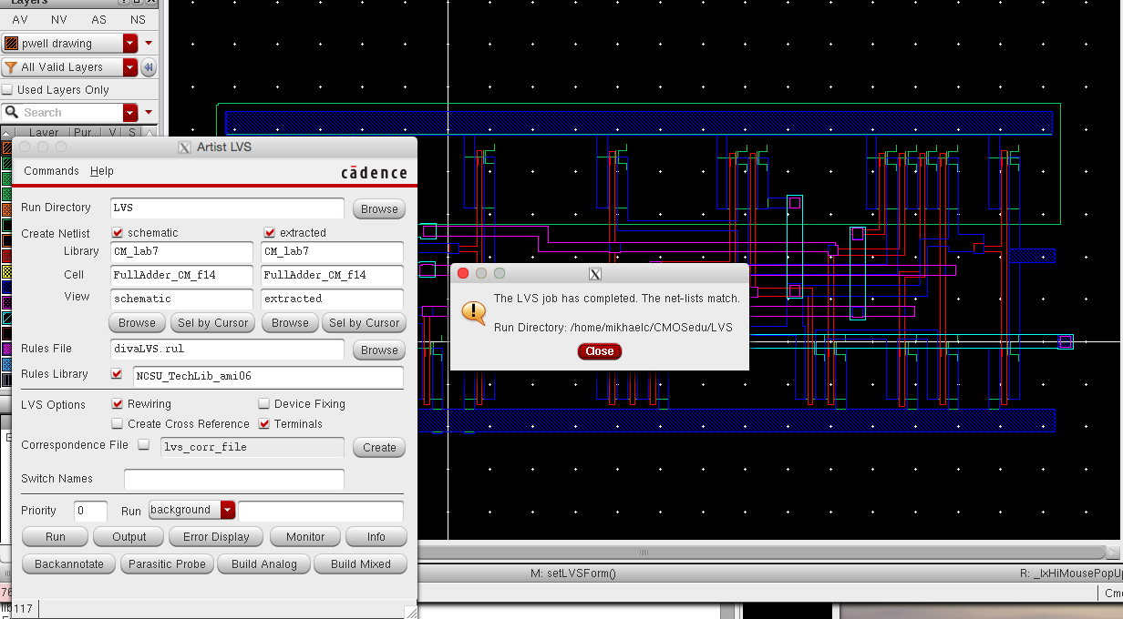
LVS was Sucessfull!!!!!!!!!!!
| Simulation Schematic |
Simulation |
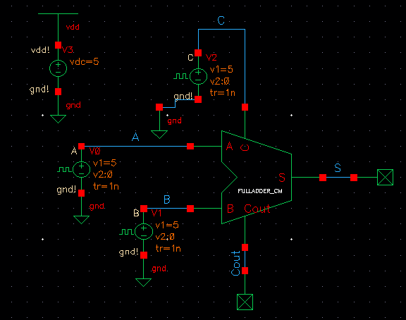 |
 |

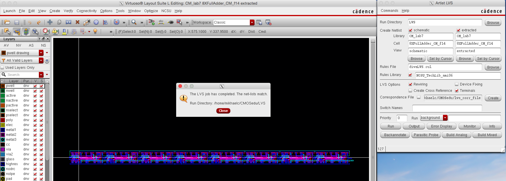
LVS Completed and match !!!!!!!!!!!!!!
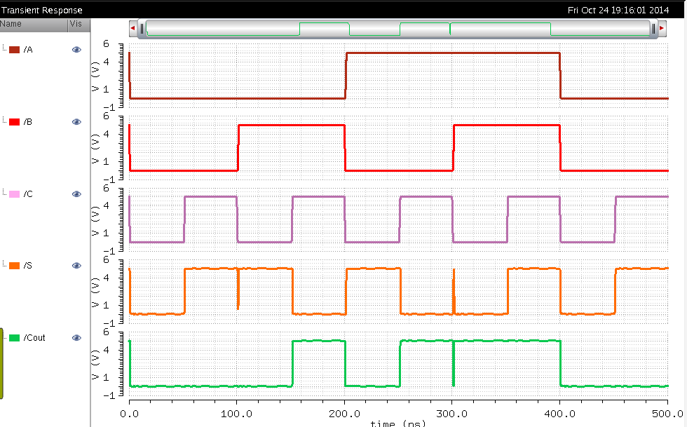
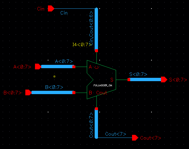
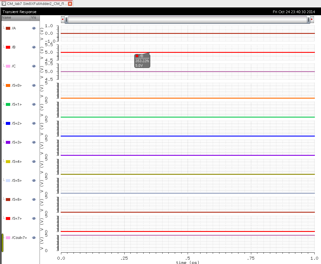
Simulation Schematic of 8 Bit Full Adder(Adding A=00000000 +B=11111111 +C=1)
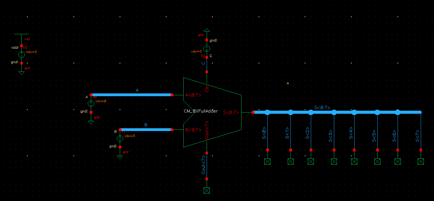
To simulate this we can place any 8 Bit numbeer into A and B but to keep things simple I added A=00000000 +B=11111111 +C=1.
The results should be as follows
Carry over 1 1 1 1 1 11 11
Carry Bit
1
A 00000000
+ B 1 1 1 1 11 11
1 00000000
Carry SUM
This is shown below in the Simulation:
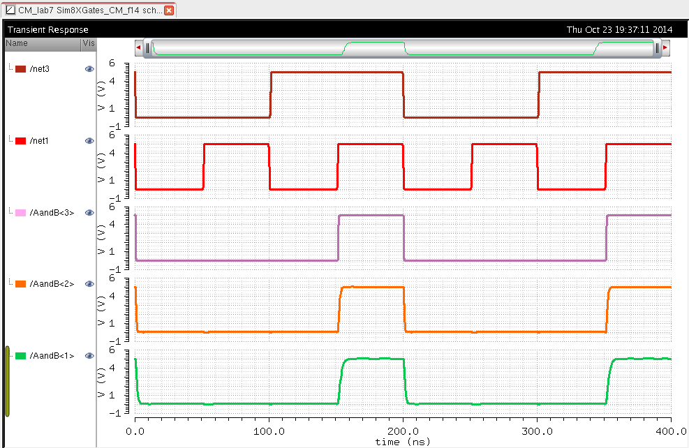
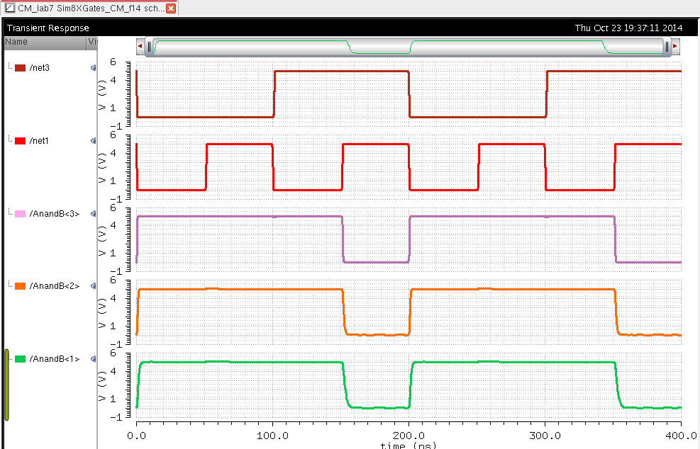
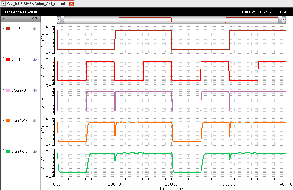
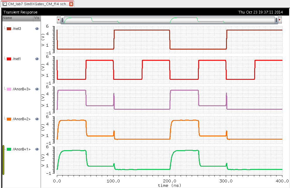
Lab 7 directory: CM_Lab7