Lab 6 - EE 421L
Objective:
The objective of this lab is create the schematic layout and symbol for a NAND, XOR and Full-adder. These devices will be used to build upon on another and will be useful in other labs. So we will need to create a standard fram for all components to sit in.
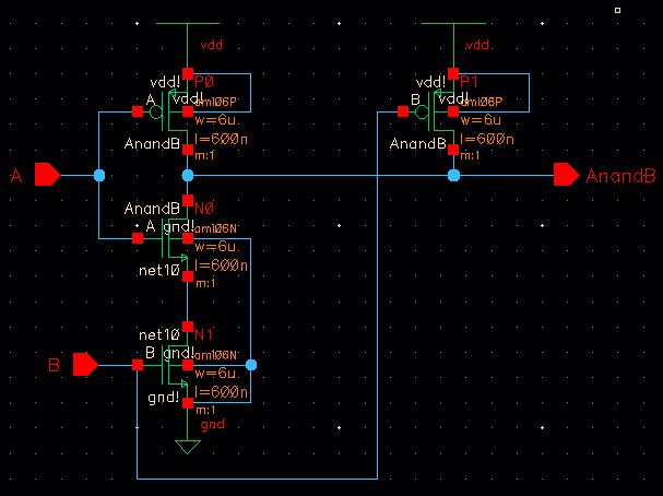
NAND:
First we will create our NAND gate. This is based off the inverter layout that we made earlier in lab5 with an extra NMOS and PMOS transistor connected. Be sure to change all the PMOS transistor to have a width of 6u. Also be sure to copy the lab 5 inverter into lab6 so that the lab 5 instance does not get ruined. The schematic is shown below:
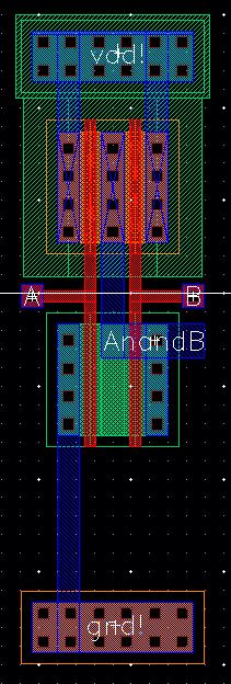
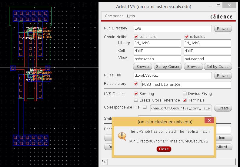
After creating the symbol we then create the layout of the component. This step might have to be revisted to fix the wireframe of the component after making the XOR. Be sure to label pins correctly, extract the layout then LVS. This is shown below:
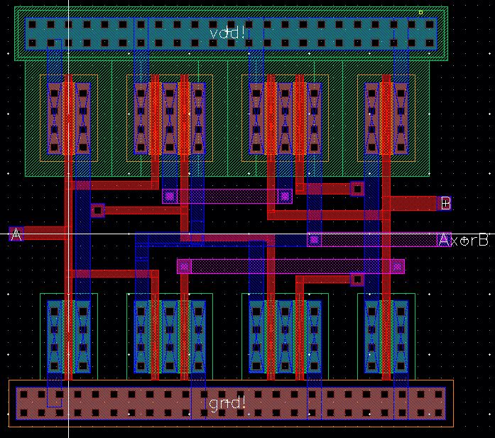
XOR Gate:
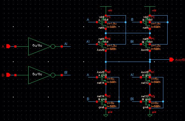
Now we will work on creating our XOR gate. This is made using the schematic below. Be sure to change all PMOS to 6u. If you are using the instance of the inverter you copied for the layout also be sure to change the symbol name as well as the PMOS to reflect the change.
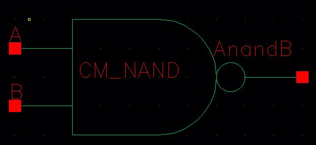
The symbol for the NAND gate is shown below:
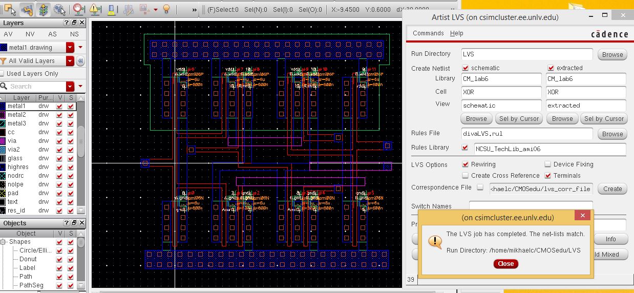
Next we must create the layout for this circuit this is done through overlapping metal connections so that the metals do not touch one another. Also note that we can stack via connection by placing an m1_m2 with and m2_m3 metal connection. This proves to be helful in a few situations. Also be sure to DRC after every few connections made to make sure that the design rules match. This is shown below:
After this is all done we then extract the file and compare it to our schematic through an LVS:
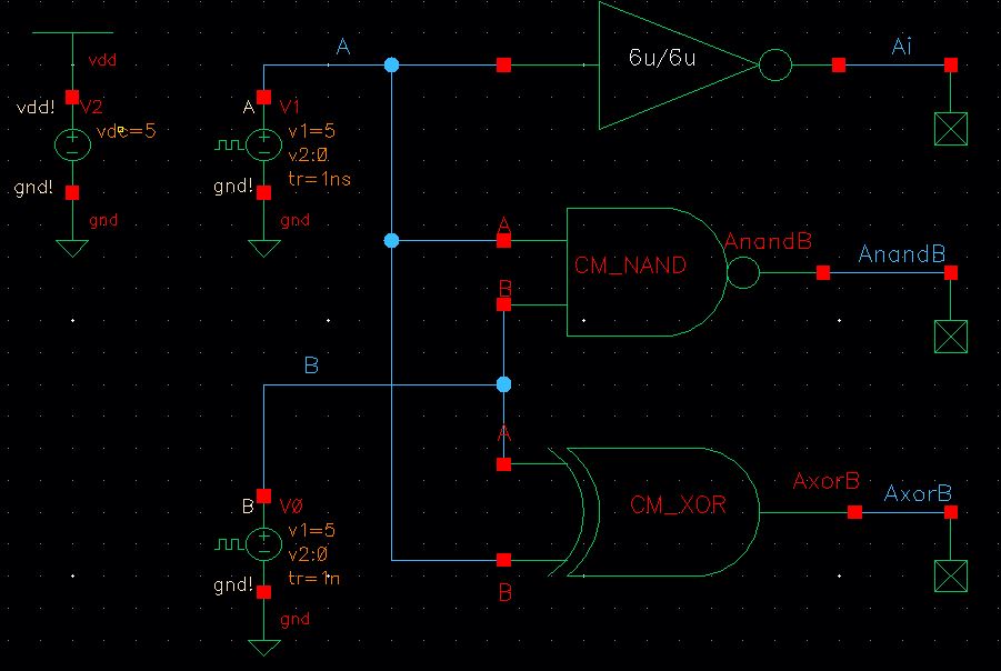
Now that this is all done we can now create the schematic and simulation to demonstrate the function of an XOR gate and the NAND gate shown above. This is shown below:
| Schematic | Simulation |
 | 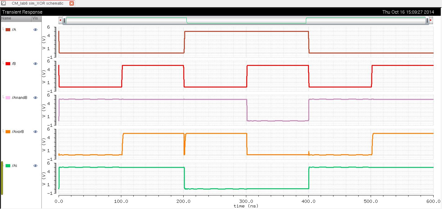 |
Full Adder:
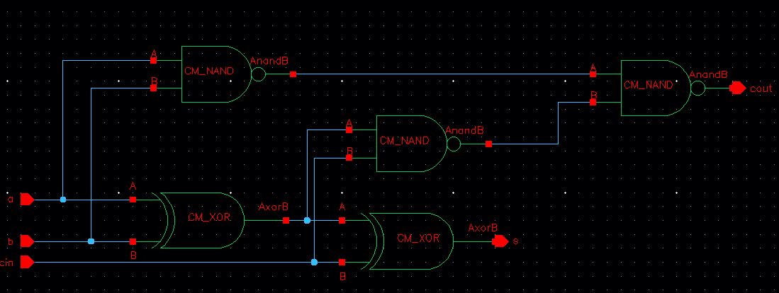
For creating the full adder we will be using both the NAND and XOR gate created above for both the schematic and the layout. The Schematic is shown below:
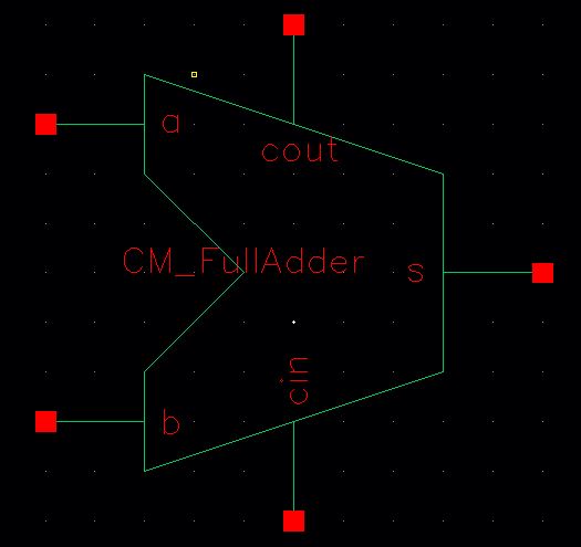
The symbol for the full adder is shown below:
After this is created we can create the layout this is done by placining the components made earlier togoether and making the proper connections to the devices. At this stage it will be usefule to use metal 3 to pass through the components. This is shown below:
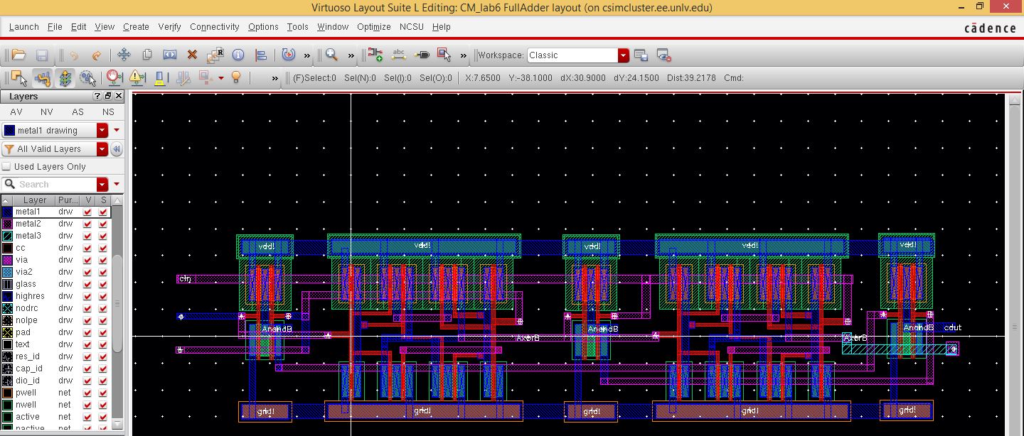
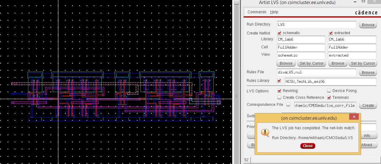
After creating the full adder we must then extract and LVS.
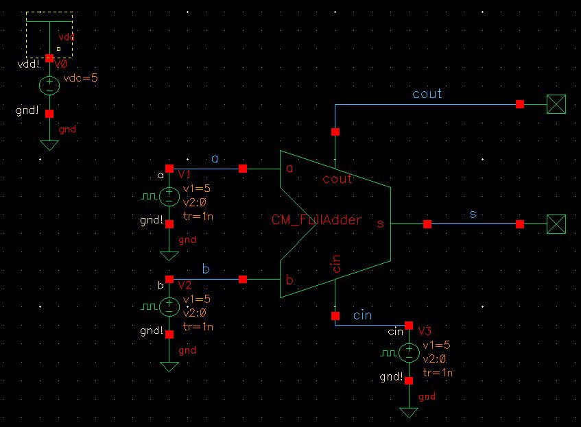
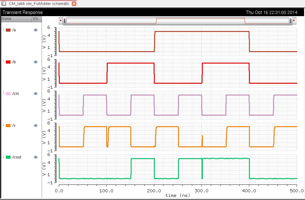
After this is complete we can then create a schematic to test our full adder and simulate the results shown below:
| Schematic | Simulation |
 |  |
Lab 5 directory: CM_Lab6