Lab 5 - EE 421L
Objective:
For this lab we are designing two inverter circuits using an NMOS and PMOS device. After these devices are layed out and LVSed we will then create a schematic with different capacitor values to view the effects different sized capacitors have on the inverter.
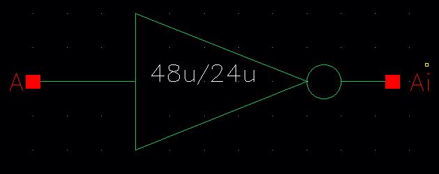
Creating a 12u/6u inverter and the 48u/24u inverter.
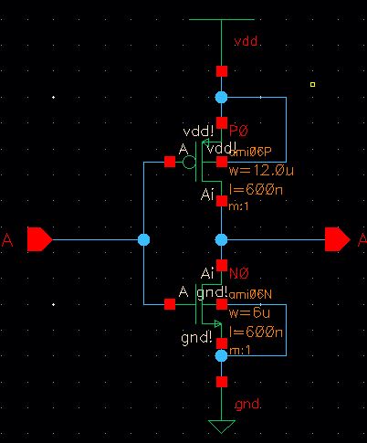
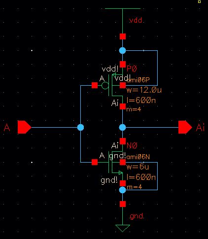
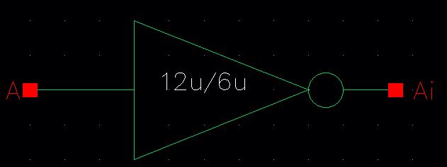
To create this schematic we put a PMOS and an NMOS together. We used a PMOS of width 12u and an nmos of width 6u. This is important becuase it balances the two transistors so they are equal and opposite. We also created the symbol for these schematics so they can easily be used later. For the 48u/24u we used the same circuit as before except used a multiplier to symbolize 4 pmos and 4 nmos transistors connected together. This is more efficent then actually creating the 8 transistors manually. This is shown below:
| 12u/6u inverter | 48u/24u inverter | |
| Schematic | | |
| Symbol | | |
After creating the proper schematic and symbol we then move on to making the two layouts. This is done by first creating the instance by going to NCSU_TechLib_ami06 and adding both the PMOS and NMOS devices being sure specify the correct width for each. We then perform the same operation for the 48u/24u but we incluce the multiplier to the schematic. This creates 4 nmos devices and 4pmos devices connected together. Next we will have to add the voltage and ground to the circuit. This is done by placing an ntap as VDD for the PMOS transistor. Be sure to use 2 rows of contacts and generous amount of columns. This ensures a good connection. Next obtain a ptap from the same library and place it next to the NMOS device. This will be our ground. The naming convention used for the ground and Vdd is gnd! and vdd! all in lower case. This makes it easier to connect to these pins in schematics. We then create the correct connections between the pads as shown below:
| 12u/6u inverter | 48u/24u |
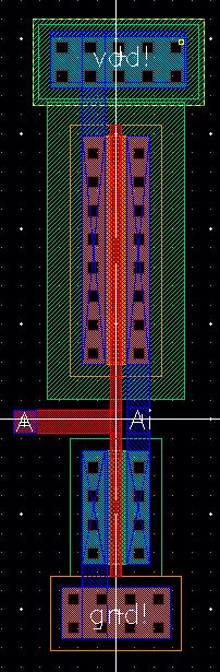 | 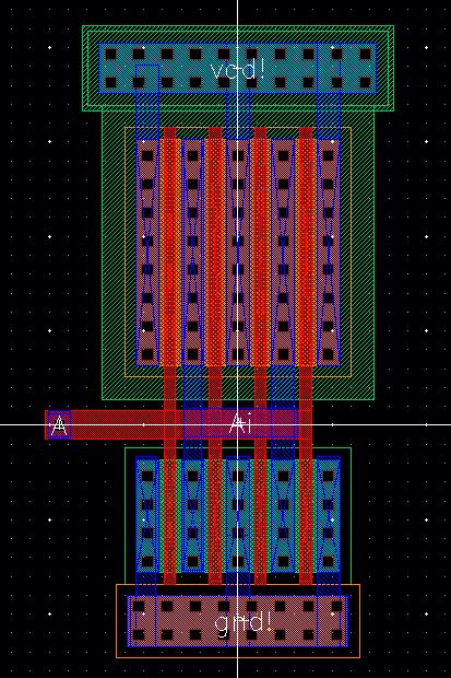 |
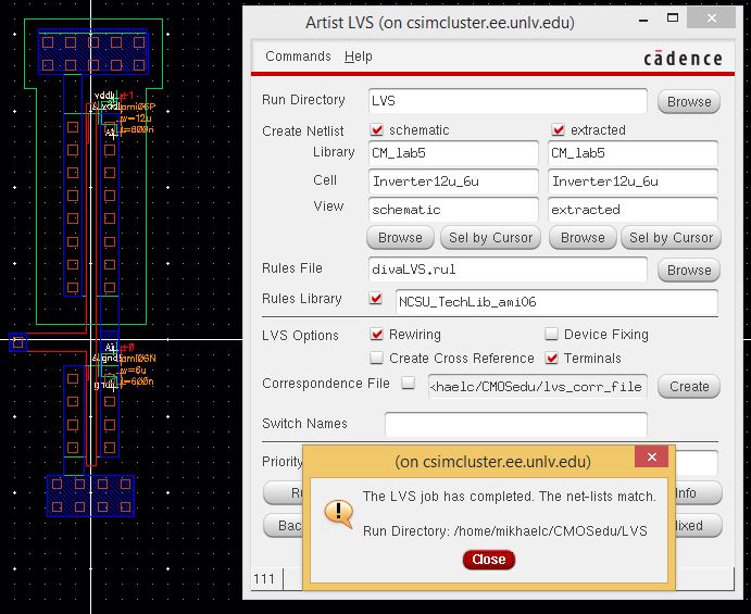
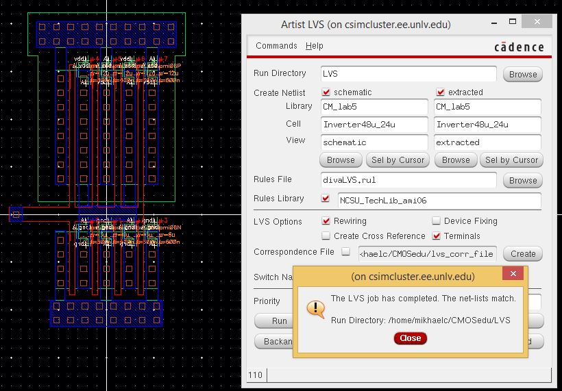
After making the proper connection extract both the layouts so they can be LVSed. This is done below:
Simulations
Simulations were performed to show how the inverter responds to different capacitive levels on the two different inverters. The simulations were also performed again using the Ultrasim functionality which helps create fast transient simulations at the expense of quality simulations. The results are shown below:
Graphs for the 12u/6u inverter using spectre:
| Schematics | Simulations | |
| 100f | 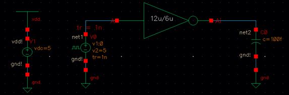 | 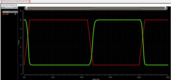 |
| 1p | 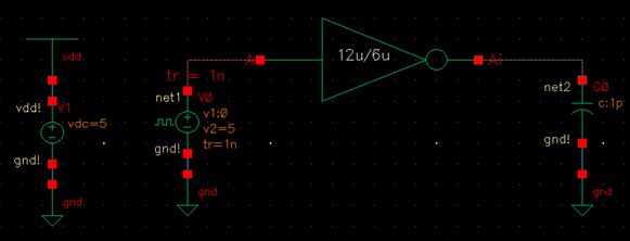 | 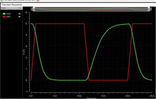 |
| 10p | 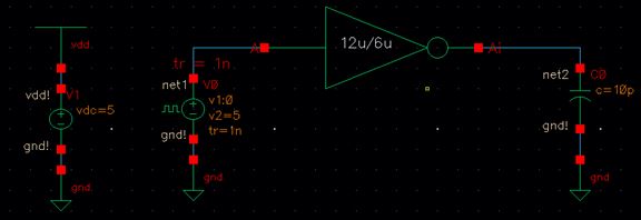 | 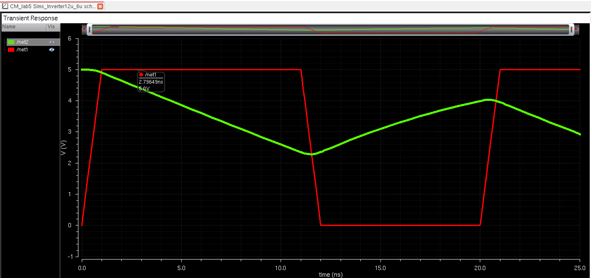 |
| 100p | 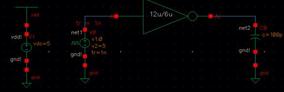 | 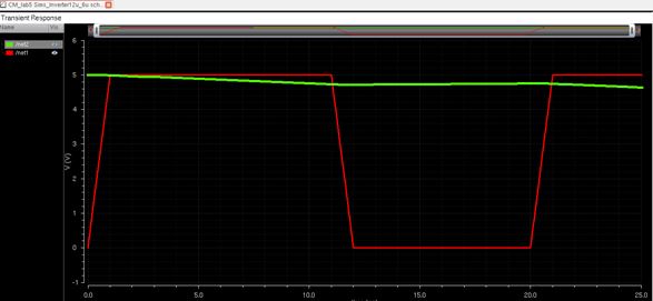 |
| Schematic | Simulation | |
| 100f | 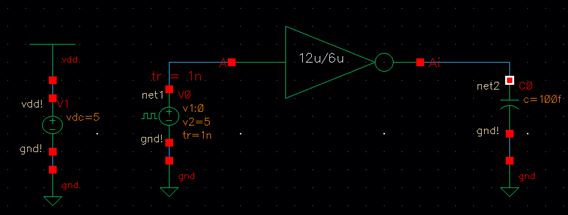 | 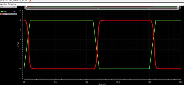 |
| 1p | 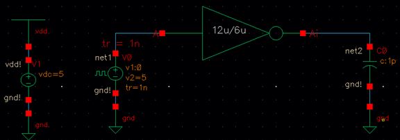 | 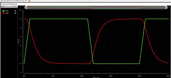 |
| 10p | 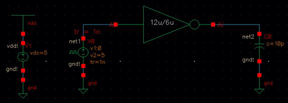 | 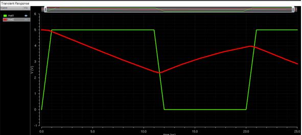 |
| 100p | 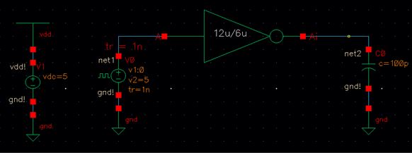 | 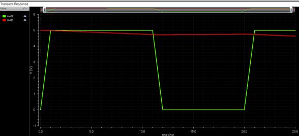 |
These simulation are very similar to the spectre simulation, but seems to contain as many data points as spectre which is more percise. But for this application it is suitable to aquire data using the ultra sim because the results are the same for the two methods of simulations.
Next we will look at the 48u/24u inverter with varying capacitance:
| Schematic | Simulation | |
| 100f | 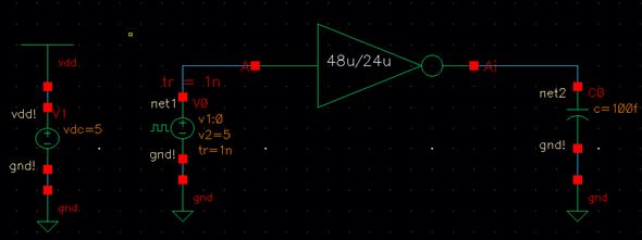 | 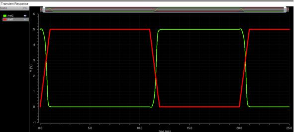 |
| 1p | 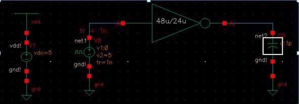 | 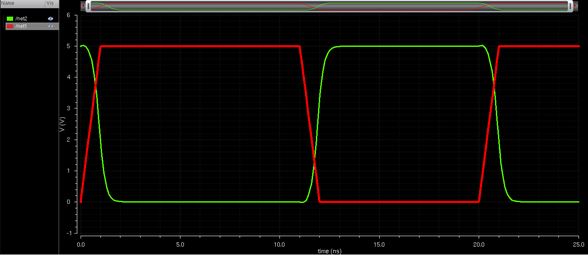 |
| 10p | 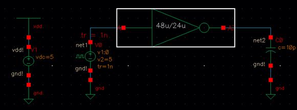 | 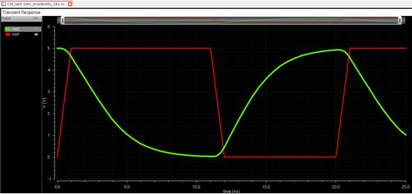 |
| 100p | 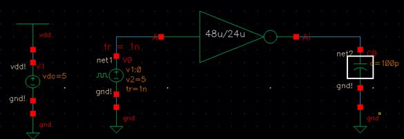 | 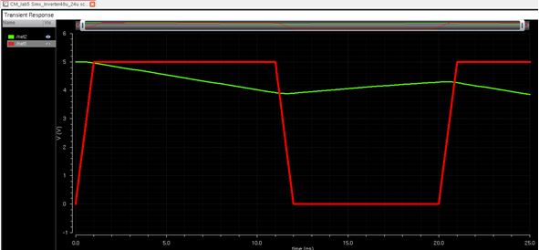 |
| Schematic | Simulation | |
| 100f | 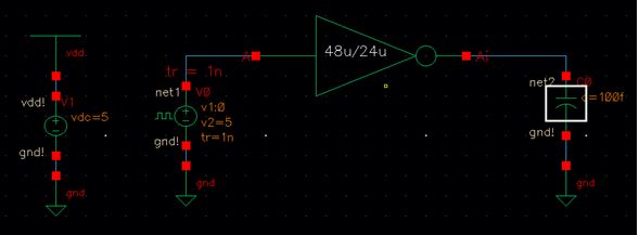 | 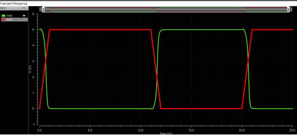 |
| 1p | 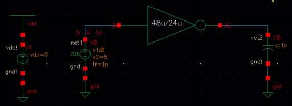 | 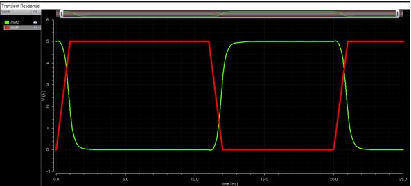 |
| 10p | 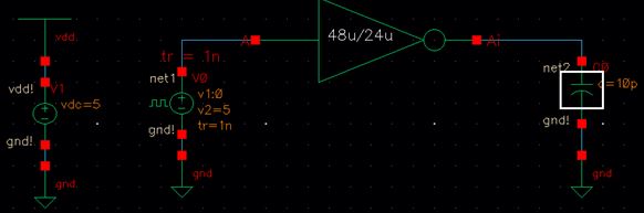 | 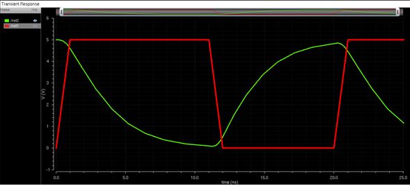 |
| 100p | 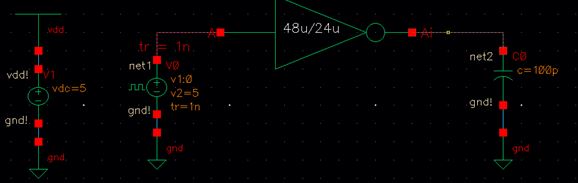 | 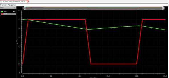 |
We can see that the fast sim shows a less smooth simulation than the spectre alternative. This is very negligable in this application. When using transient analysis the Ultrasim is a good alternative to spectre as long as the data is not datapoint intensive.
Lab 5 directory: CM_lab5.zip