Lab 3 - EE 421L
Authored
by Christopher Mikhael,
Email: Mikhaelc@unlv.nevada.edu
9/17/2014
The objective of this lab is to use Tutorial 1 to help create a layout for the DAC bit created in Lab2.
We
will begin this lab by laying out a 10K resistor. To perform this we go
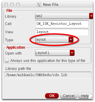
to our library manager and create a new cellview. Be sure to
change the type of the cell view to layout, to specify what type of
file you will be making.
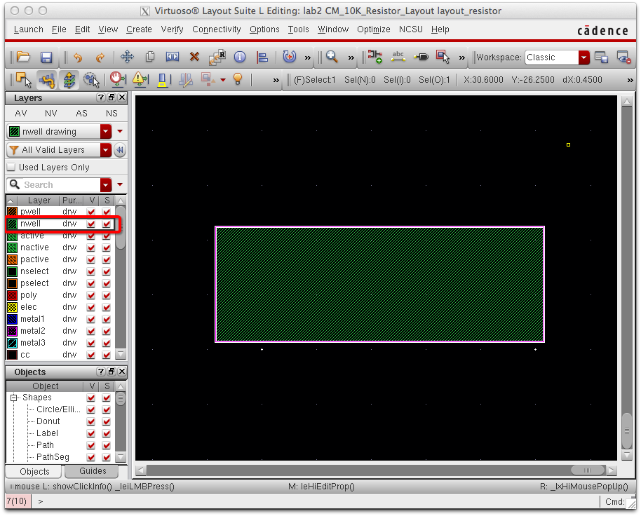
No
enter the layout file and select nwell on the left panel. Then go to
Create>>shape>>rectangle or use bindkey r. Then drag and
create a rectangle on the screen of any size as shown below:
Calculating Resistor Values
We
can now edit the demensions of our rectangle. To do this we need to
know some of the design rules for the C5 process in MOSIS.
The
resistance for a square in mosis is 800 ohms. This value can be used
for all simulations. For an indepth look at all the paramaters for
Mosis click the following link: MOSIS ami C5
To find the parameters of other processes go to: http://www.mosis.com
Under sheet resistance it will show the ohms/sq for different layers.
For Nwell it is 801 ohms/sq which can be approximated to 800.
Now that we know our sheet resistance of the Nwell layer we can start calculating the W and L. This is done using the equation:
Rtotal=R/sq(L/W)
So to obtain a 10K resistor we can do the following:
10K=800(L/W) where
L or W can be designated as an arbitrary value to find the other value.
To choose the correct width keep in mind that for N-well
it must be larger than 12 lamda.
Since lamda is 300 nm this value is 3.6 microns.
To meet this criteria we will use a length of 56u
10K=800(56u/W) therfore W=4.5u
Another
issue that arises is that since Length and width are arbitrarily
selected they may not snap to grid with the values obtained.
The snap spacing for Cadence is set to .15 microns. So
all values used should be divisble by .15 microns and produce a whole
number. The value of .15u can be found and verified by creating a
marker and ruler to show where the grid snaps.
To verify our values we can take 56/.15 = 373.3
For this example we will round the number up to 374 and multiply by .15 to obtain our new length=56.1
The same is done for width: 4.5/.15=30 therfore the number meets Cadence standards.
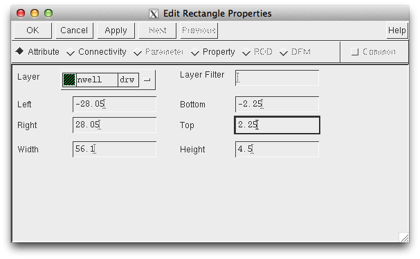
To
create and center our rectangle in the center we will divide the value
the length and width by 2 and place the positive and negative values in
the property section of the rectangle (found by pressing q).
Now that we have done the math we can put these values into the window generated when pressing q as seen below:
This
layout should be able to DRC at this point. Go to verify>>DRC and
press ok when the window is opened. Make sure there are no errors.
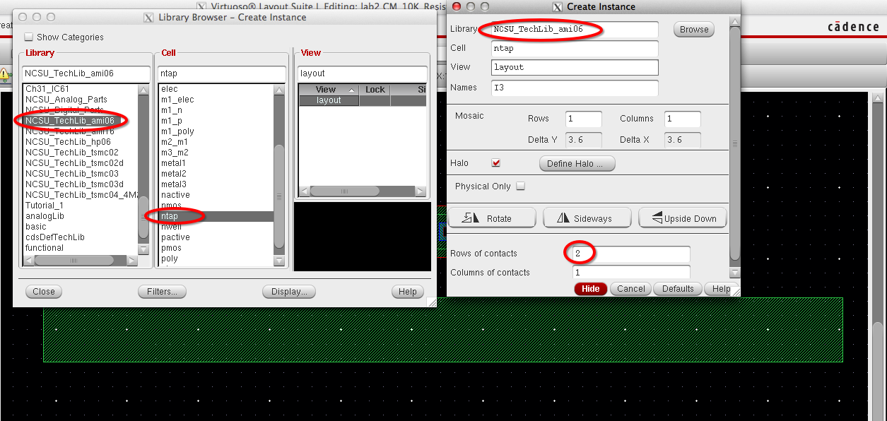
Next
we will add the metal connections to the ends of the resistor. To
perform this press the bindkey i and find the ntap cell shown below.
Also add another contact to the rows of contacts so that the contact
fits the rectangle created.
This
will allow you to put down two square red connectors. To change the
look of these connectors press e to open display options. Change the
display levels so that they stop at 10. Now adjust the connectors so
they match the rectangle. The resistor should look like this:
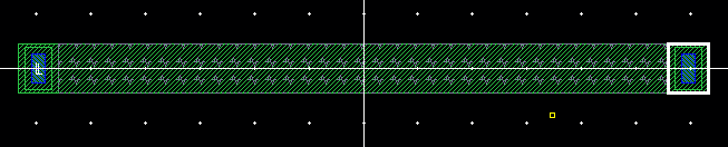
Now we need to add pins to the layout. To do this we can select metal1
on the left panel. Then go to Create>>pin. Here we need to diplay
the name of our pin and we will call it L:
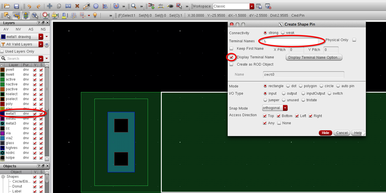
After selecting the pin draw a rectangle around the metal 1 connection and place the name of the connector onto metal 1.
Do the same to the other connector but name it R.
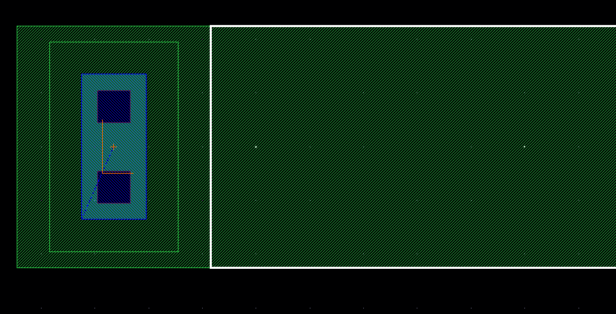
Next select res_id from the left pannel then use the rectangle tool and
highlight the body of the resistor without the ntap connectors.
The result should be as follows:
Now we should verify that there are no errors and find the approximate
resistance of our layout. First DRC the resistor and make sure it
passes all the checks. Then go to verify>> extractor and extract
the file. This will create a new file in the cellview of your project.
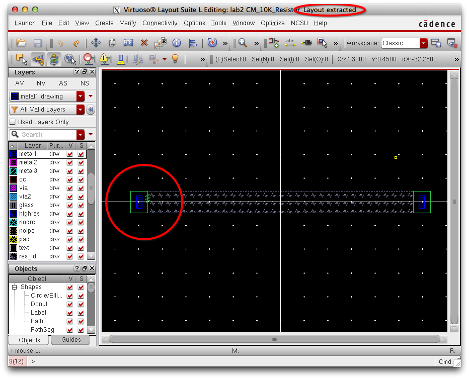
Save and close the layout and then open the extracted version of the
layout found in the library manager. Once in the file zoom in to left
side of the ntap resistor:
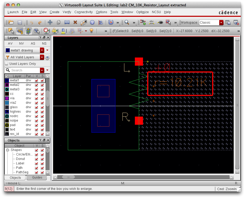
As we can see below our resistor is a 10.21K resistor.
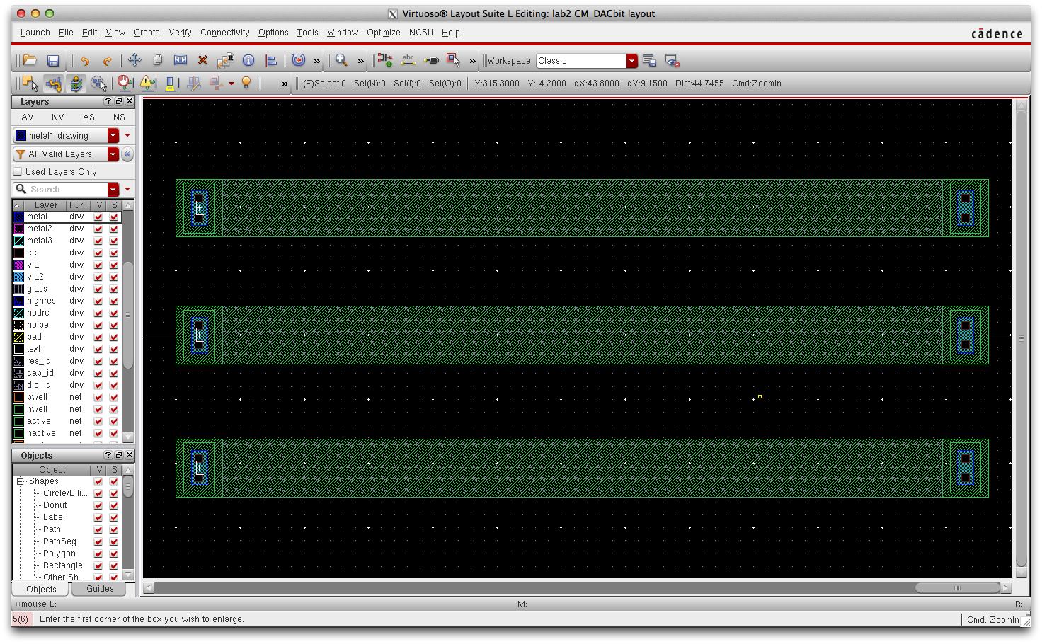
Now that our resistor is finished and saved we can use this in the
layout of our DACbit. First go to the library manage and create a new
cellview under the DACbit created in lab2. Make the new file a layout.
Open this file and press i. Browse for the resistor layout which was
just made previously and select it. Place three of these resistors
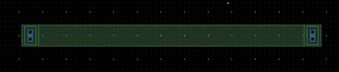
right under each other. It should look like the following:
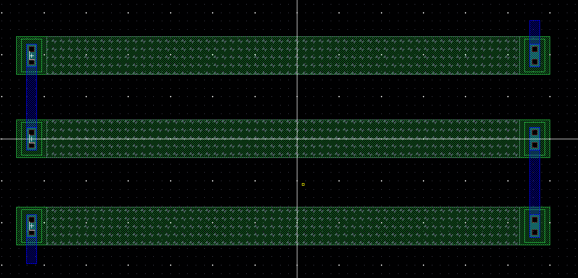
Next we will create the metal connections between the three resistos to
create the voltage divider created in our schematic. To do this select
metal1 in the left panel use the bindkey r to create a rectangular
shape stretching from one metal node to the the other. Also create an
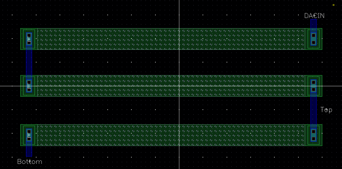
input and output metal connector. The layout should look like this:
Now we will need
to add the name of the input and output pins. This is done by selecting
create pin and highlight the metal node using the rectangle tool. After
all the pins are named the layout should look like the following:
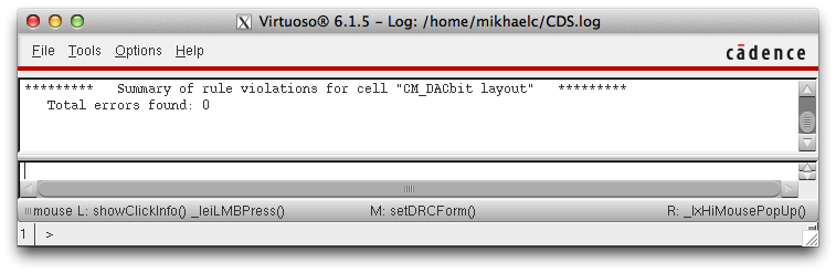
After this is complete DRC the layout to ensure all spacing meet the C5
process requirements.
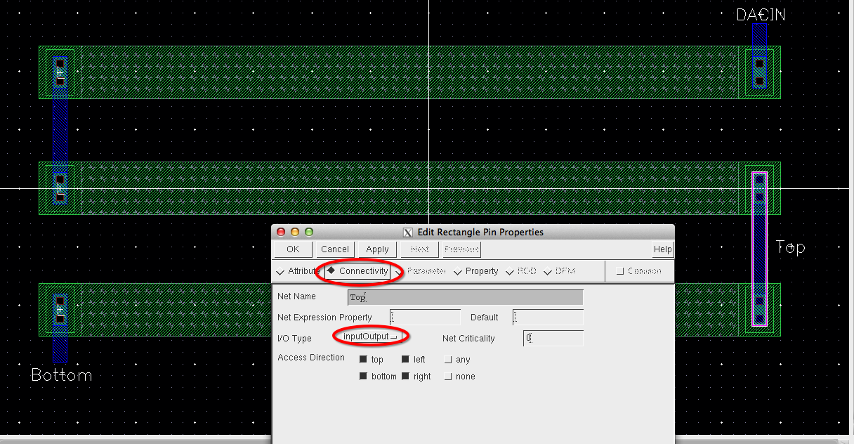
To LVS the system we will need to first extract
the layout by going to verify>>extractor. After this is
performed we can LVS our layout. After pressing Run wait for the LVS to
finish, press the output button in the LVS window. This will provide
you with a textfile showing all errors. The main error in this lab was
mismatching inputs with input/output. So we need to insure that each
input types are the same in both the schematic and the layout. To
change these types use the bind key q to view properties. Then click on
the connectivity tab and choose the correct I/O type.
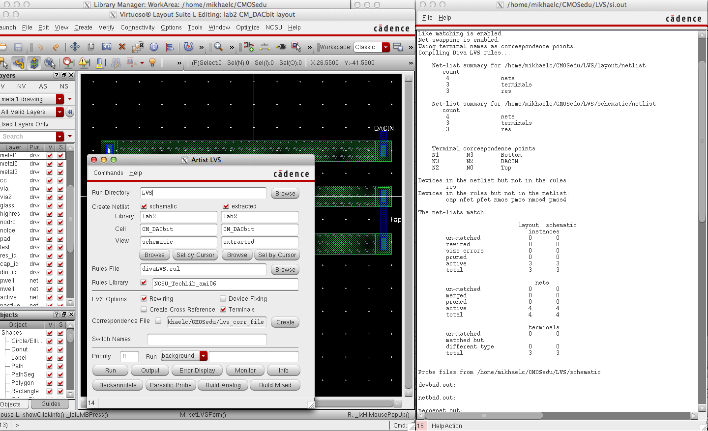
After the pins are set to match the schematic we can extract and LVS again. This time there should be no errors as shown below:
This concludes the lab. To view the actual layout files click here: CM_lab3.zip