Lab 2 - EE 421L
Authored
by Christopher Mikhael,
Email: mikhaelc@unlv.nevada.edu
9/6/2014
Pre-Lab
First Download lab2.zip which containst the ADC and DAC files
Place this file into the CMOSedu directory and unzip the file
After this is complete we must edit the cds.lib file to include lab 2
- Open cds.lib file
- Add the following command
- DEFINE lab2 $HOME/CMOSedu/lab2
Then start Cadance from the CMOS directory using
virtuoso &
The Library manager will appear. Go to lab2 and select sim_Ideal_ADC_DAC and select the schematic.
The following schematic will apear:
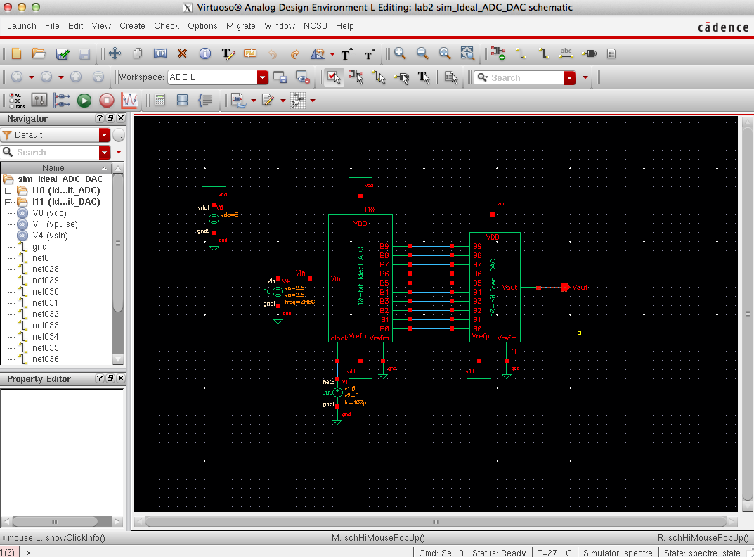
Then Run the simulator by going to: Launch >> ADE. Once the ADE is open makesure that the simulator is on spectre.
Then go to: Session >> Load State >> Cellview
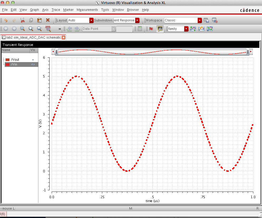
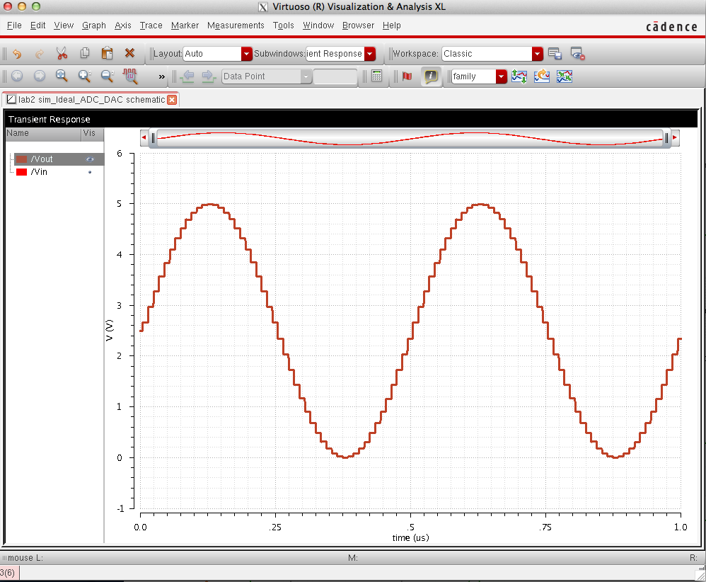
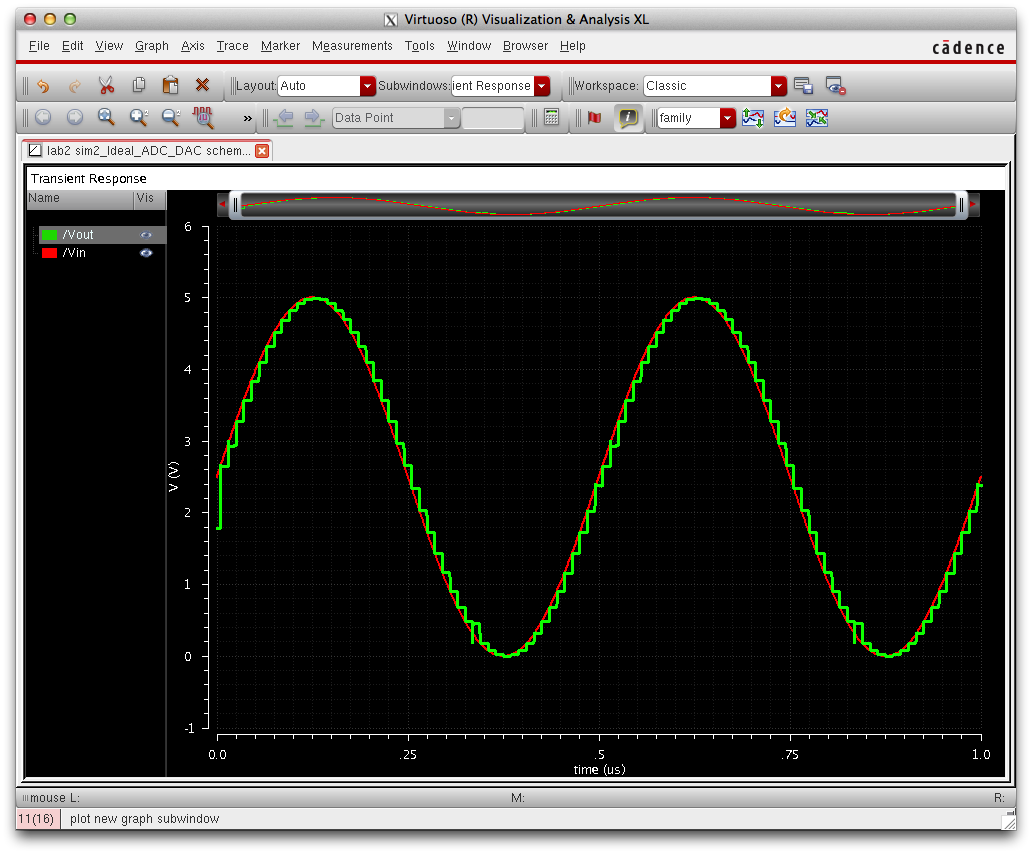
The following graph should be obtained:
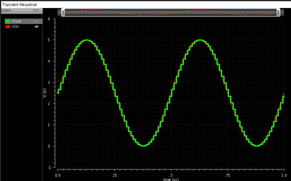
As you can see the analog smooth signal is sent to the ADC where it
becomes a digital signal that is then reconverted into an Analog signal. When the signal enter the DAC the Digital
signal is summed together to provide the digitized analgo signal. The square wave shown above is an analog singal with less sampling because a lot of values are lost during ADC.
This is better seen when seperating the two waves:
Analog
|
|
Analog after Conversion
|
 |
|
|
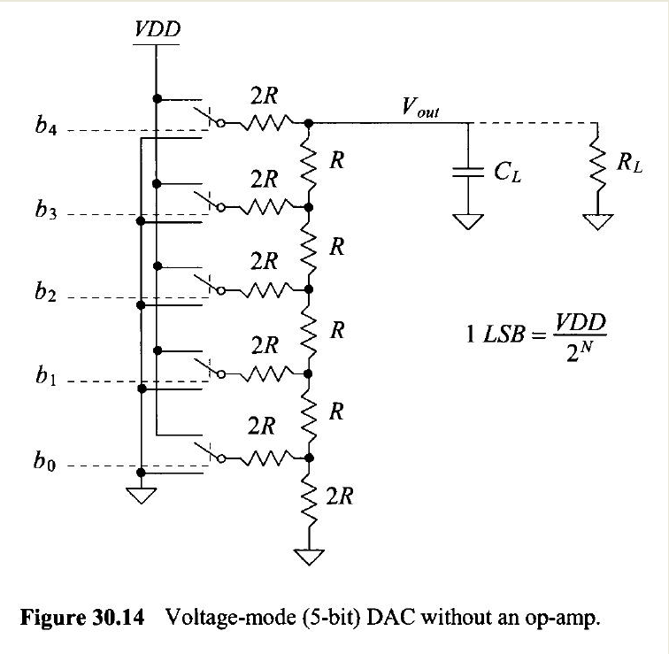
The least signigican bit can be found by taking VDD and dividing it by
2^(bits). This will show the approximate increase of each step which in
this case is 5mV.
The equation is as folows: Voltage=((Input signal)/(2^(bits)))*VDD
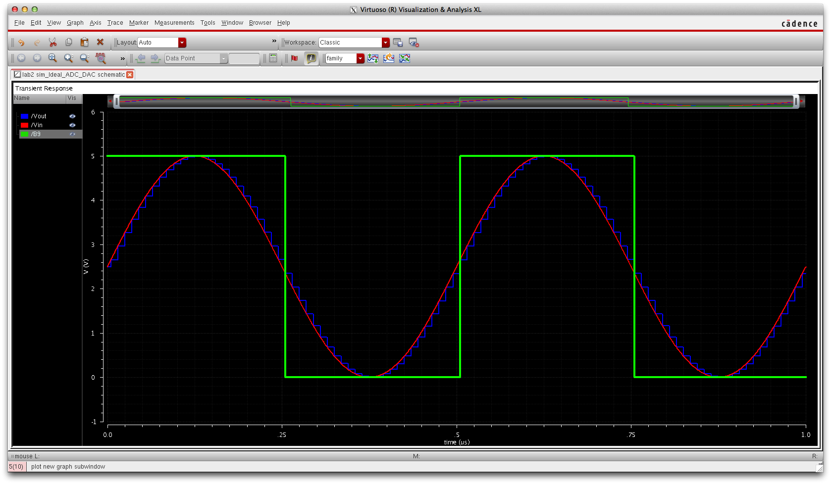
Below B9 is shown compared to the input and output. We can see that
this acts as a binary input when the voltage is above/below 2.5 volts
the signal acts as a
binary switch turning on/off.
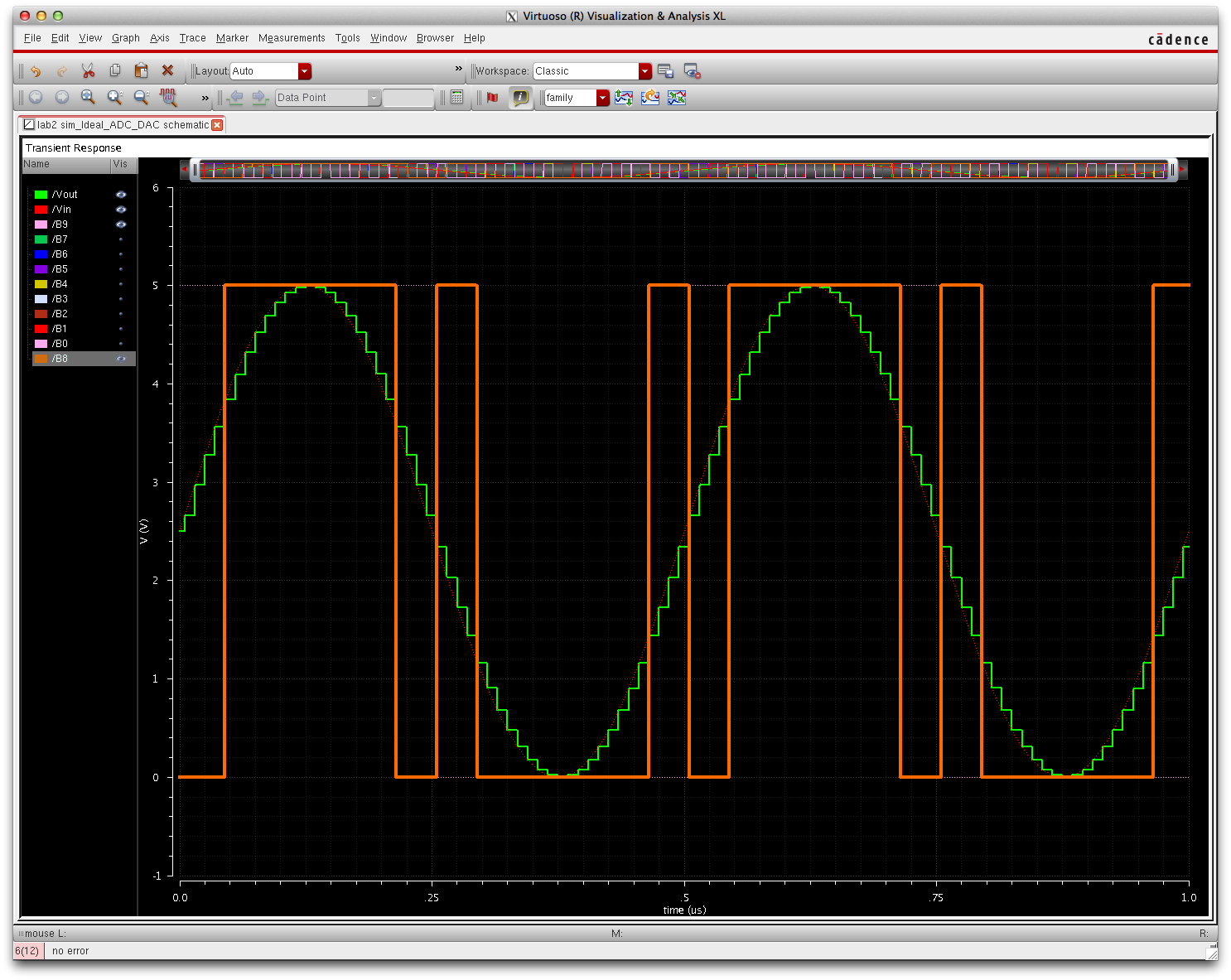
When we look at B8 we see that the on off voltages change to 3 points.
The signal chages from on to off at the 1.25V mark 2.5 mark and the
3.75 mark.
For the values B7-B0 the voltages at which the signal switches from the
on state to the off state become closer and closer producing the step
discrete analog
signal shown above in blue. This pattern continues to repeat until each step is accounted for at B0.
PostLab
The objective of this lab is get familar with editing schematics and
viewing them in different heiarchies and symbol views. This lab deals
with an ADC to DAC converter
where we must change the curicuit underneath the DAC to the following:
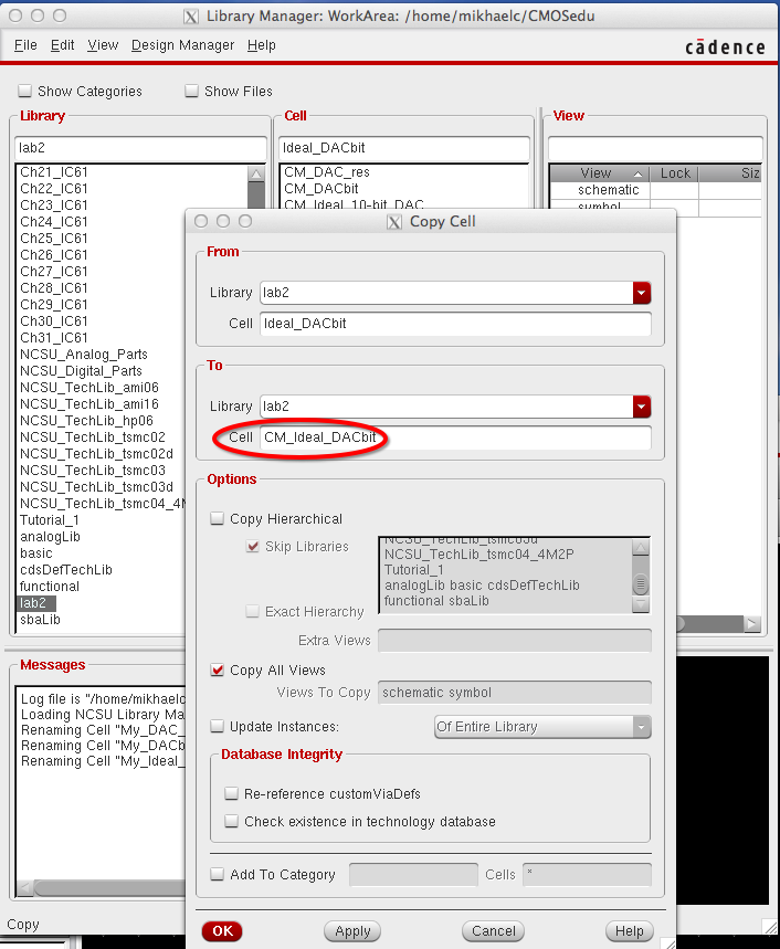
To perform this we will first create copies of the schematics already
provided in Lab 2 so to have a safepoint back for reference. To copy
file into the directory of the file manager right click and select copy, then change the name
of the file.
We will first copy the Ideal_Dacbit which is the lowest level of the DAC component.
Now open the newly created DACbit file. Delete all contents of this
file. We will be creating a voltage divider for the circuit in figure
30.14. We want to make it so that the circuit can be used to create the
entire 10bit DAC. So we will have two 10k resistors for one branch of
the voltage divider and one 10k resistor. Use the bindkey
p to go to the pin creation menu. Enter a name for the pin and select
its function. Then place the pin on a branch of the schematic as seen
below:
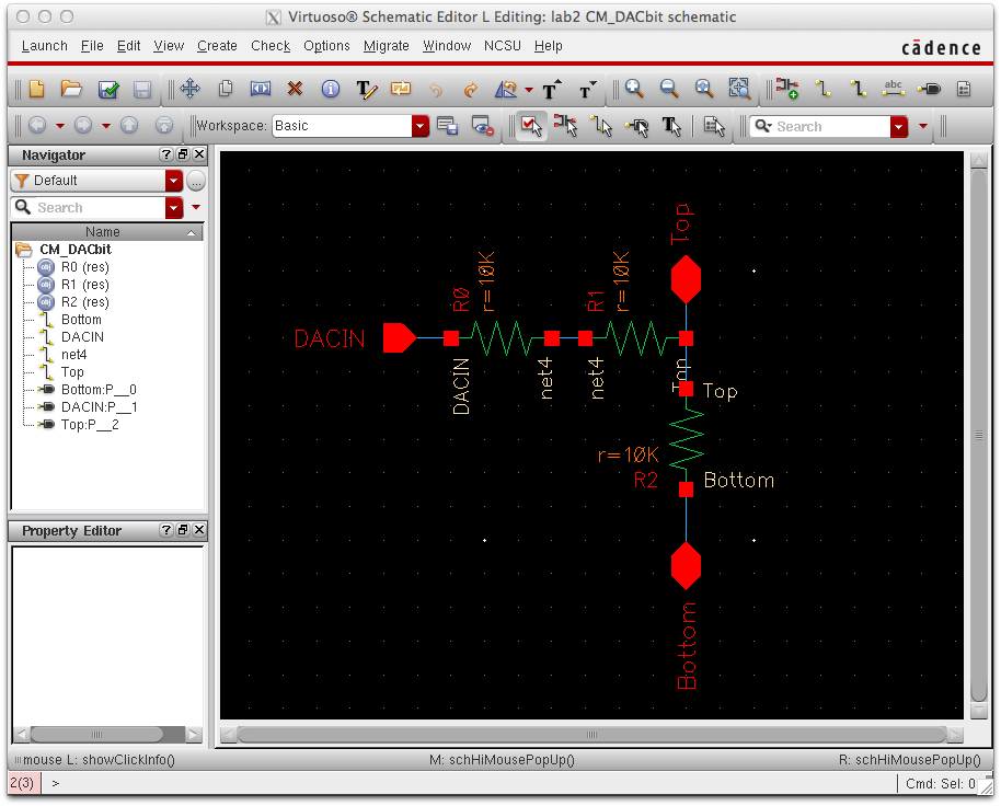
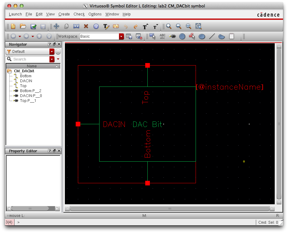
Once the schematic has been created press the check save button and
make sure no error occur. After this step we will want to create a
symbol for this component. Go to Create >> Cellview >> From
Cellview. Then press fix any issues with the direction of the inputs
and outputs and press ok. A symbol will apear in a new schematic winod.
Here we can edit the symbol to our liking. Once complete save check the
file.
After this is complete close both the schematic and symbol being sure to have saved both documents.
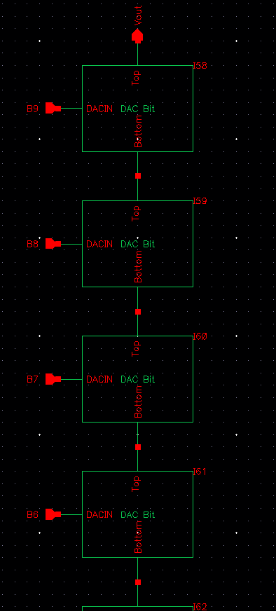
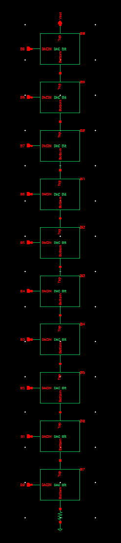
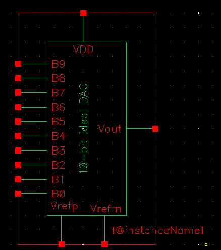
Next we will copy the Ideal_10-bit _DAC. In this schematic also delete
all the items. Within the schematic press bindkey i and go to the
component browser. In the browser find lab 2 in library. Then select
the DAC bit which was created earlier. We will need 10 of these
components. Once they are placed connect them from top to bottom and
connect a 10k resistor and ground on the last DAC Bit. We will then
need to place the input and output pins for the schematic. Place a Vout
pin (Bindkey p) at the Top of the first DAC bit. Then we will name each
DAC in from B9 to B0.
Once
this is completed save and check the work and resolve any errors.
Since we copied the Cellview we can go into the symbol already premade
and eidth the inputs and outputs to match our schematic. To do
this all we have to do is remove the VDD, Vrefp and Vrefm. This helps
us create a symbol under the same footprint as the one before.
BEFORE
|
|
AFTER
|
|
=>
|

|
After saving and checking close out of both the symbol and schematic.
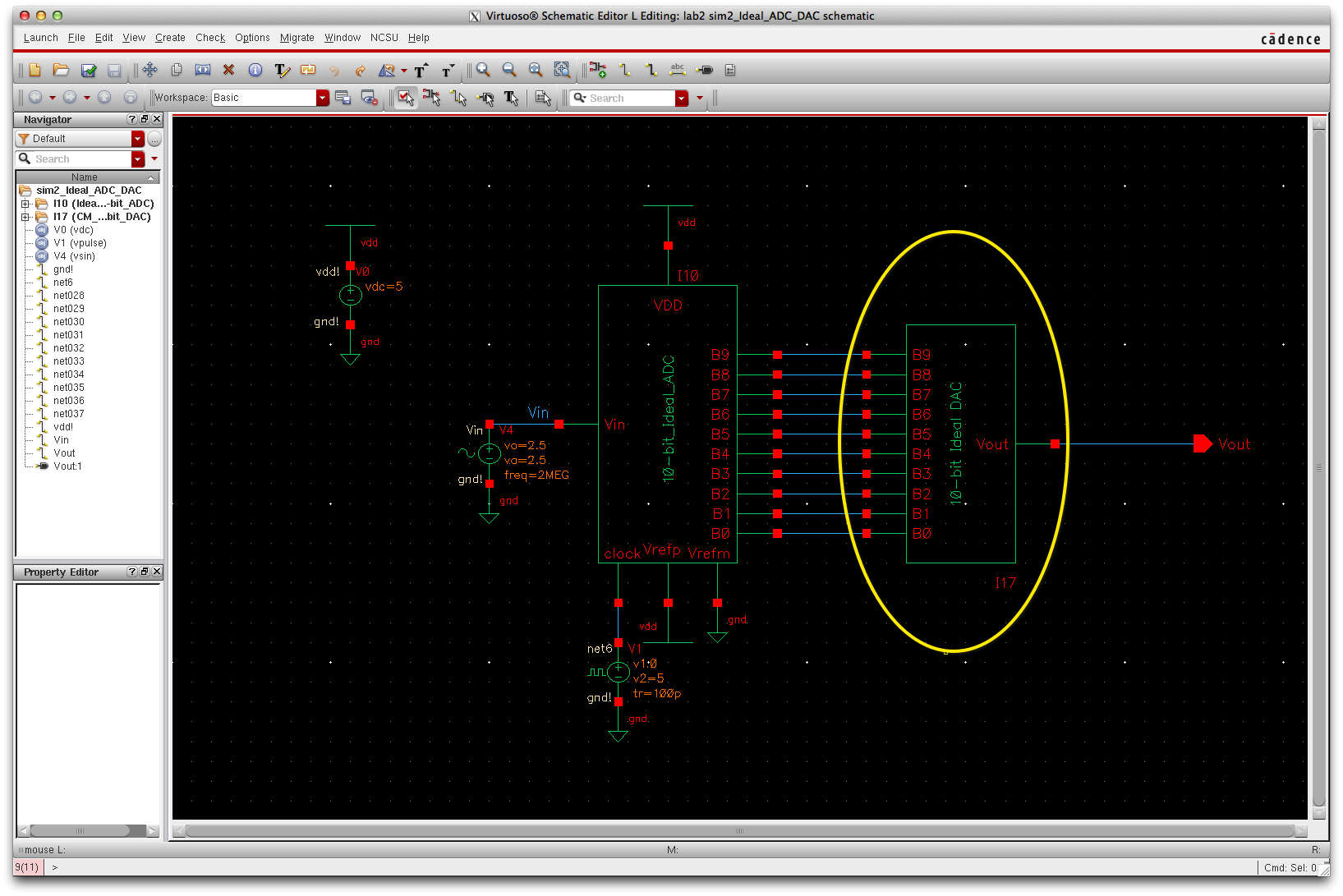
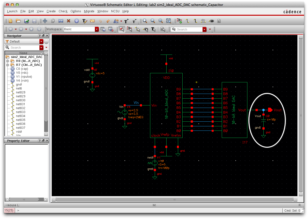
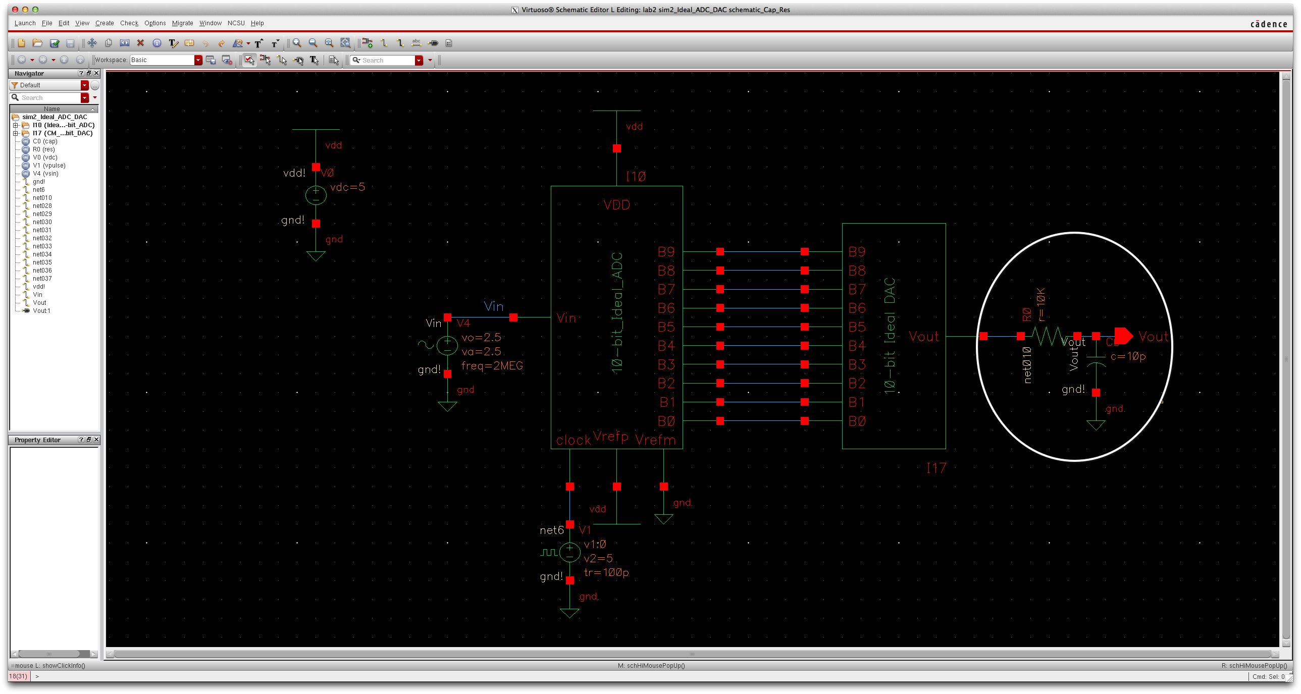
Next we will copy sim_Ideal_ADC_DAC and name it sim2_Ideal_ADC_DAC.
Once the schematic is open we can delete the old DAC component and
replacing with the new one created. This is added using the component
browser and selecting the new Ideal_10-bit_DAC file. When component is
successfully placed, select the component and press bindkey x. This
should bring you into the 10-bit_DAC schematic. One can also click on
the DAC bit and use the x bindkey to view the schematic of the voltage
divider. This should be to done to make sure all files are properly
placed. To go back use the bindkey b.
Simulations
To create a simulation go to Launch>>ADE L in the schematic window.
Once in the simulation window. Make sure that the simulation is set to
spectre (should be automatic). Then go to Outputs>> To be
plotted>> select on schematic. Then go to the schematic and
choose the Vin and Vout node. Then create a transient analysis of 1
microsecond by going to Analyses Choose.
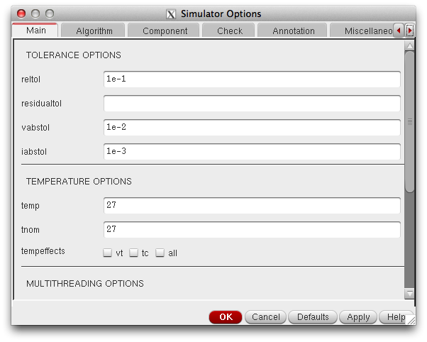
One additional step is required for getting schematics to work
properly. Go to simulations>> options >> Analog and change
the following settings:
Then save as cellview and run:
Simulation with 10K resistor:
Schematic with added 10K resistor
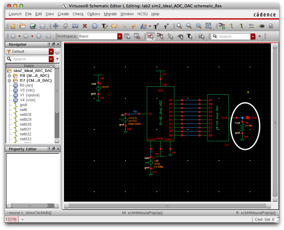
Simulation:
When adding a 10K resistive load the signal lost strength and became half of
its original output. As the load increases the singals amplitude will
get smaller and smaller. A resistor can be used in this case to control
the amplitude of the output signal. Note since no capacitance was
provided the signal had no horizontal shifts and the wave remained jagged. The Extra 10k does the following Vin(R/(R+R)) compared to Vin(R/R) which causes the signal to be cut in half.
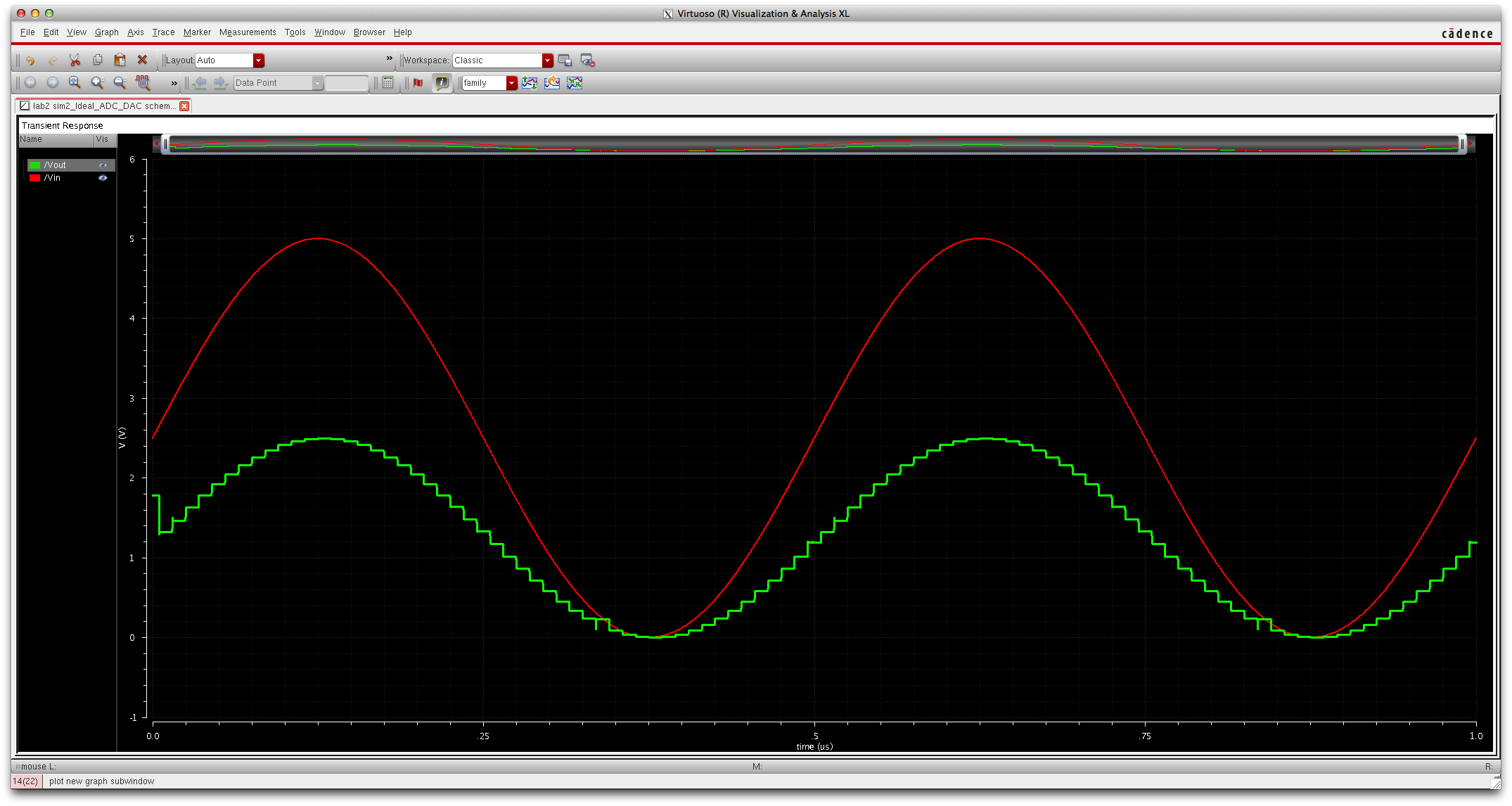
Simulation with 10p Capacitor:
Schematic with 10p Cap:
Simulation:
Adding a capacitor has two main effects on the signal. The capacitor
first off smoothes the signal making it look more like an analog
singal. Capacitors are often used to smooth out signals since they act
as a bucket which retains the electricity and allows a constant flow to
leave as shown above. Another effect the capacitor had on the signal is
an obvious phase shift. The Time delay is approximately 76ns from the
graphs shown above.
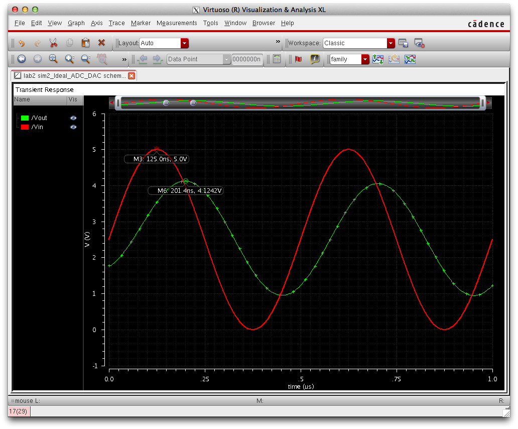
Simulation with 10K Resistor and 10p Capacitor:
Schematic with resistance and capacitance:
Simulation:
When adding the resistor to with the capacitor to the circuit we see
that the two previous simulations are almost joined to create the
above. The time delay increased from just having the capacitor. 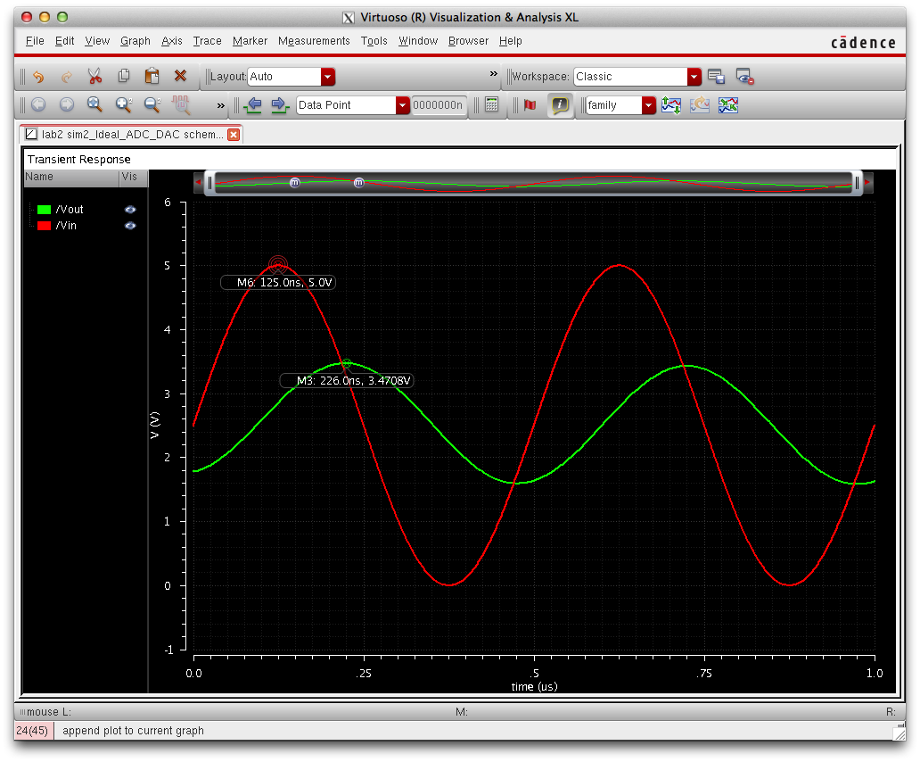
The
time delay here is about 101ns. Also we can see the amplitude of the
output is smaller than the capacitor only simulation and larger
than the resistor only simulation.
Other questions:
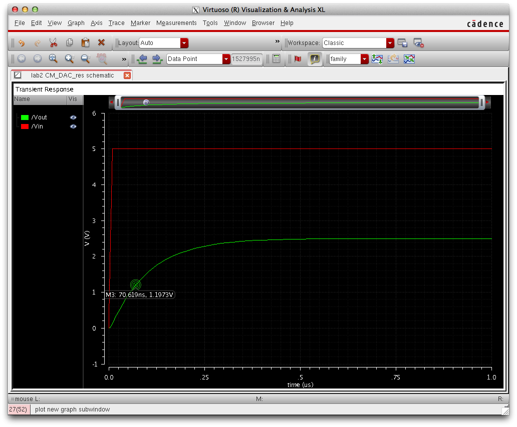
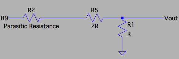
Time Delay:
To find the time delay we use the formula .7RC in which case
R=10K and C=10p. Thus the time delay is 70ns which is approximately
what is observed in the simulation below which was done by taking the
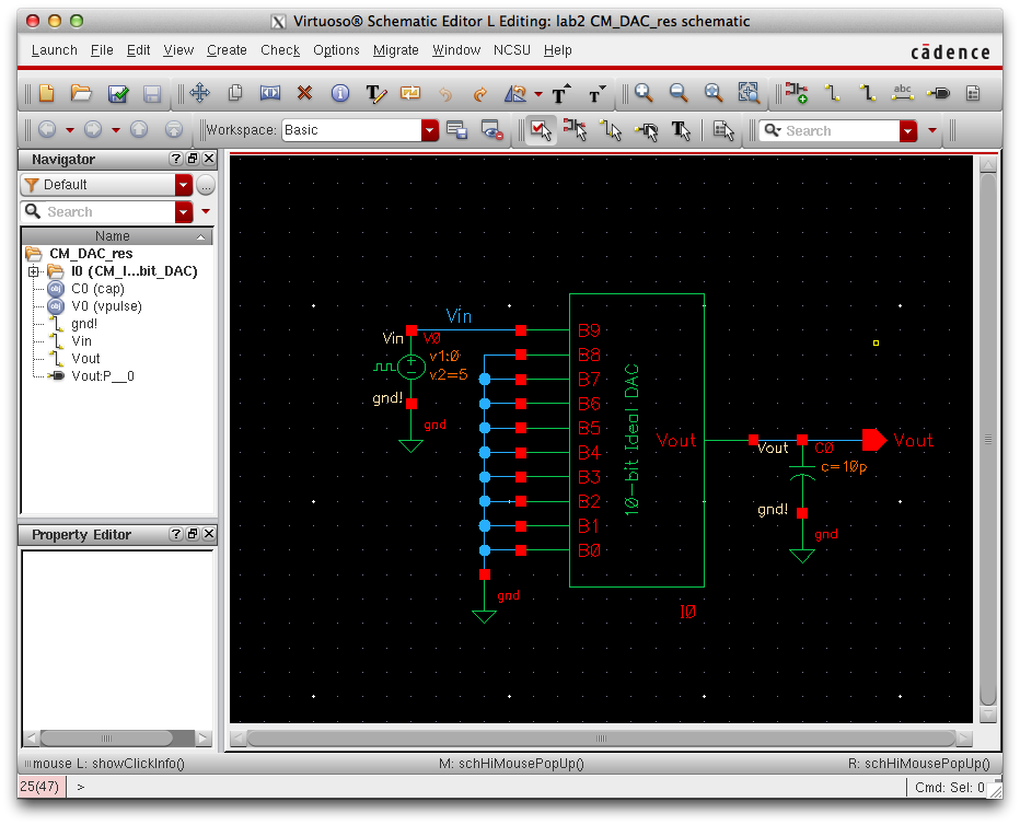
DAC bit and grounding all the inputs except for B9 which is connected
to a pulse. For Vout we add a 10pF capacitor.
Schematic of B9 DAC configuration
As we can see the time delay is about 70 ns in the simulation.
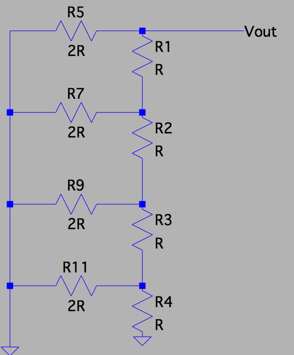
Finding Output Resistance:
To
find the output resistance we place all the inputs from B9:B0 to GND.
Then add the resistors in parallel and series to obtain an output Resistance and Vout which in this case equals R.
Modeling with transistors:
If
instead of switches, a transistor were to be used, the resistance on the
2R branch would become larger because of the transistors parasitic
resistance. This would cause the output voltage to go down because it
is changing the resistance of the voltage divider.
This Concludes the lab to view the output files please view: CM_Lab2