Project - EE 421L
Authored
by Gerald Lee
leeg28@unlv.nevada.edu
November 9, 2014
Design, Simulation & Layout of an 8-Bit ALU
Design of a 1 Bit Input/Output ALU
Schematic
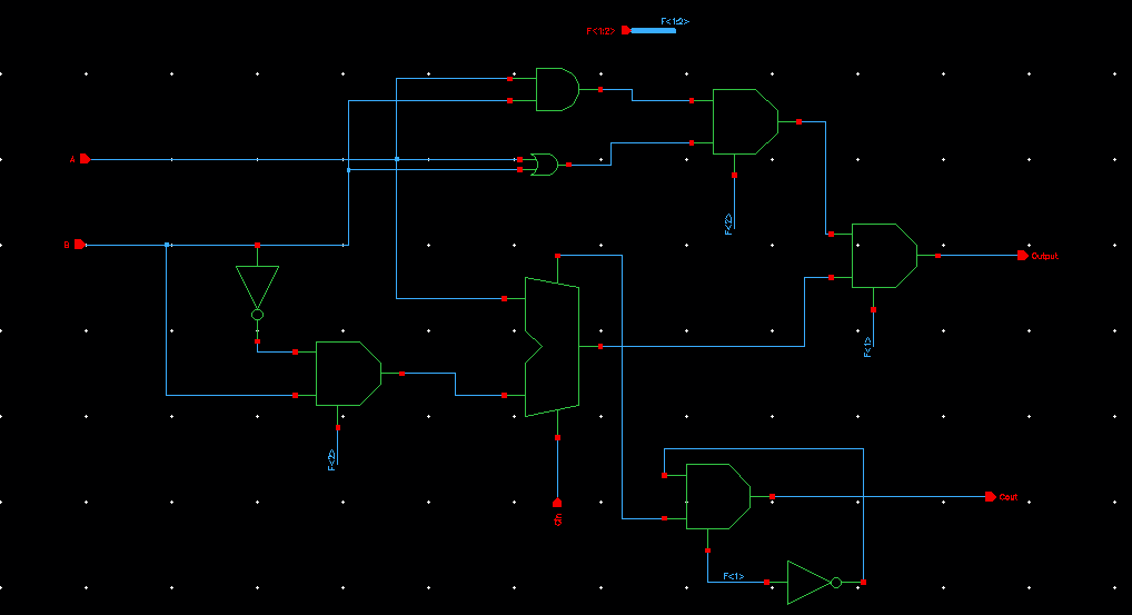
Please note that F is a 2 bit bus used for design specifications, on
the bottom right corner of the schematic you will see that included
a multiplexer with an inverter in order to set the carry out when using
logical operations to "0". Using F1 and F2 as reference ALU operation
is as follows 00:ADD, 01:Subtract, 10:Or, 11: AND. To perform
subtraction b' is added to A because of the property A-B = A + (-B).
Verification
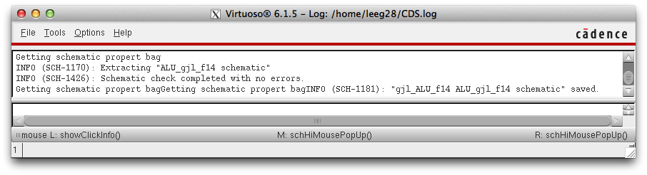
Symbol
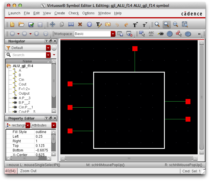
Verification:
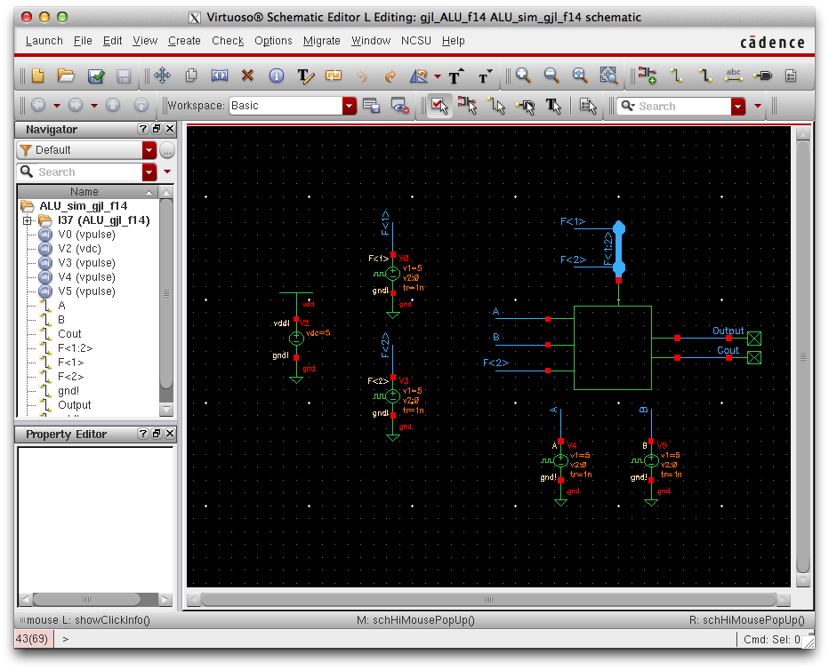
Simulation Schematic:

Simulation Results:
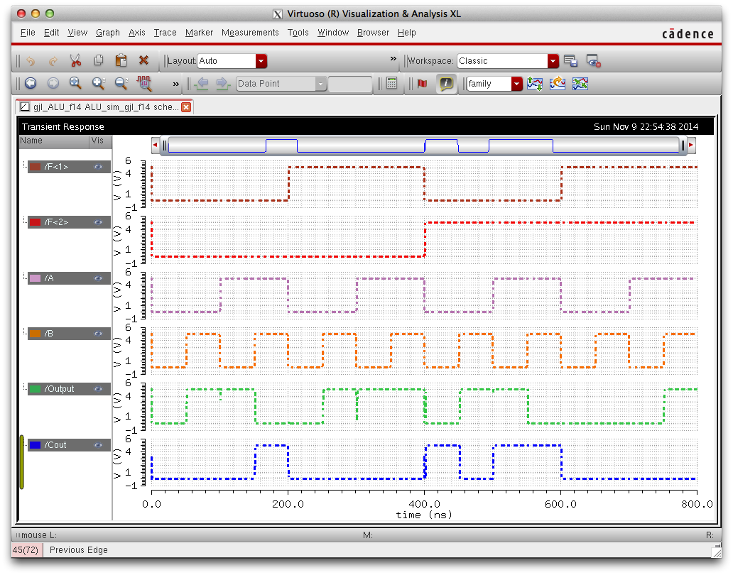
Using F1 and F2 as reference ALU operation is as follows 00:Add, 01:Subtract, 10:Or, 11: And.
The simulation split into quarters performs these operations in order 1) Add 2) Or 3) Subtract 4)And
All operations perform as expected.
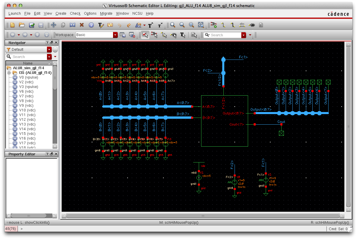
Design of an 8 Bit Input/Output ALU
Schematic:
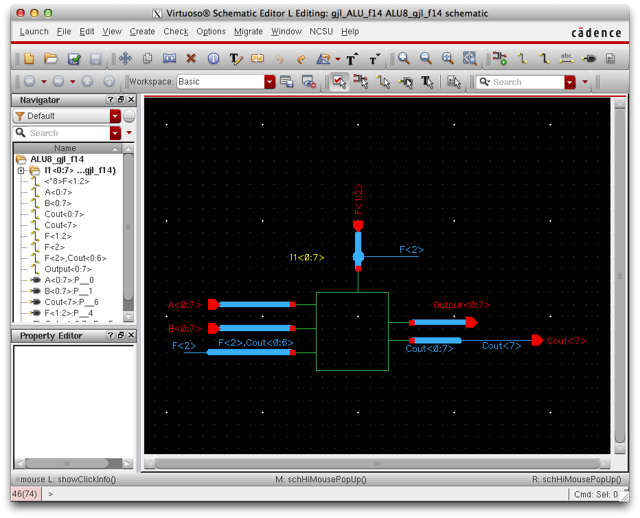
Please note that Final Design Symbol Specification stated that Pins
were to be buses, notice carry out, F<2> is tied to the
carry
in of the first ALU to have a clean Cout signal as discussed before, lastly notice that Cout is propgated through the ALU and
only the carry out of the last ALU is the only pin to be outputted.
Verification:
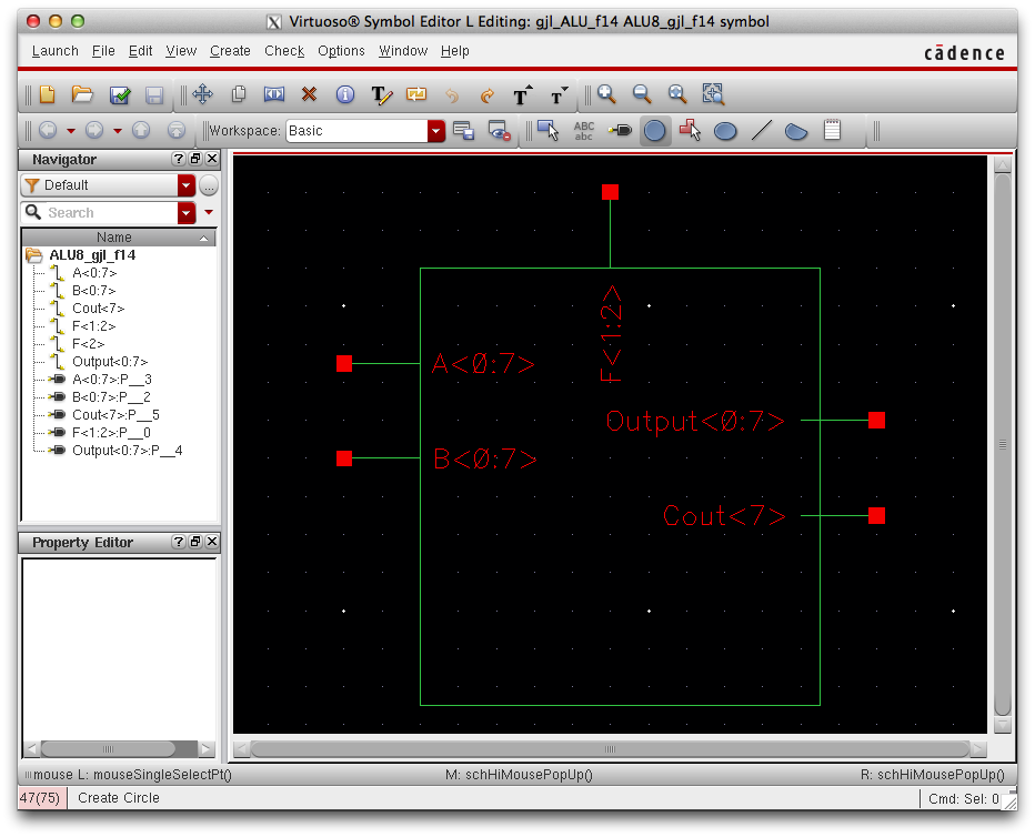
Symbol:
Verification:
Simulation Schematic:
Simulation Results:
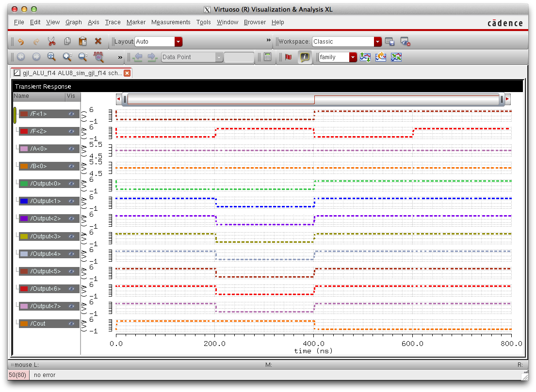
Using A=11111111 & B=11111111 as inputs notice that all
functions of the ALU still perform correctly. ALU operations using
F<1> and F<2> as refereence
as repeated from above are as follows: 00:Add, 01:Subtract, 10:Or, 11: And. To show that my 8-bit ALU was operating correctly I only plotted
one bit of A and B since the entire A & B bus is set to "1". Notice
during addition, Ouput<0> is set to O while the carry is
propagated through
Cout<1:7>. Notice that during subtraction that in two's
complement 1-1 => Cout= 1, Output= 0. Lastly notice that during And
& Or operations
Cout is logic "0".
Layout of an 8-bit ALU
Layout of a 1-bit Input/Output ALU
 Above show's my layout for 1-bit Input/Output ALU...
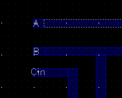
In the top left corner A,B and Cin pin's can be found...
In the middle left side of the layout F<1> and F<2> pins can be found...
In the top right corner my output pin can be found...
In the bottom right corner my Cout pin can be found...
1 Bit Input/Output Verification
DRC Check

LVS Check
Above show's LVS net-list match for 1-bit input/output ALU.
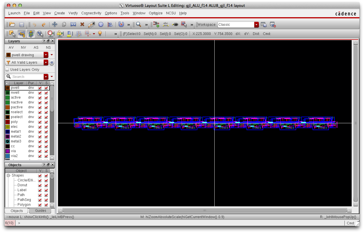
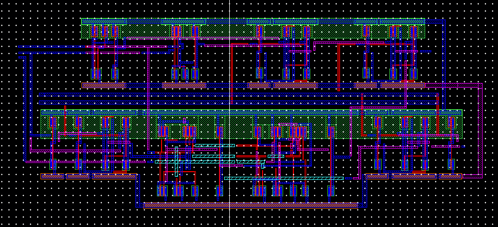
Layout of a 8-bit Input/Output ALU
Above show's the final layout of my 8-bit Input/Ouput ALU...
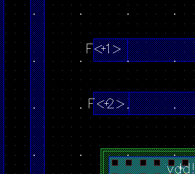
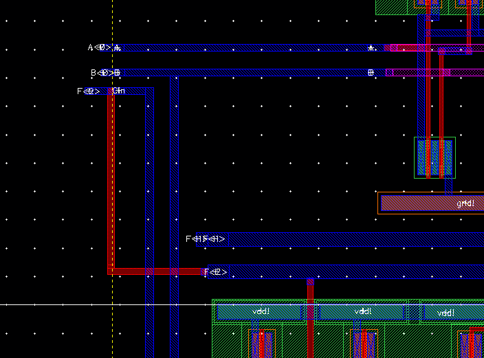
The
picture above shows the cconnections of the left side of my first ALU
cell, notice pins A<0>, B<0> and Cin. Also, notice that
F<2> is tied to Cin to match schematic of my 8-bit ALU.
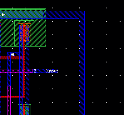
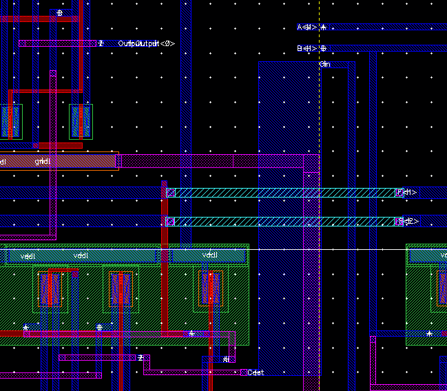
This
next image show's the connections on the right side of my first ALU
cell, observer output<0> and notice that F<1> and
F<2> are continued using metal 3 connections and that Cout is
tied to Cin, these connections are duplicated in between each ALU cell
except for the last....
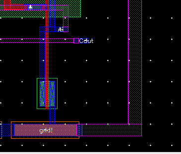
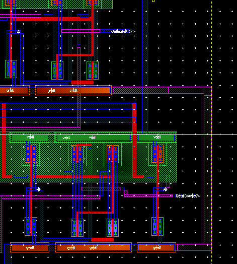
The
next picture show's the right side of my last ALU cell, notice that
that last Cout pin (Cout<7>) is not being tied to Cin and is
being displayed as an output.
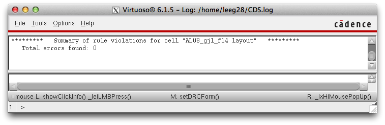
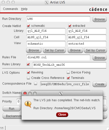
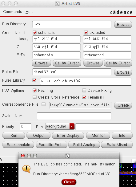
8 Bit Input/Output Verification
DRC Check
LVS Check
8 bit ALU LVS check passes!
This concludes the lab project...
As always back up your work!
NOTE to grader: Please use cells "ALU_gjl_f14" and "ALU8_gjl_f14" for LVS Checks
Design Files can be found here...