Project - EE 421L
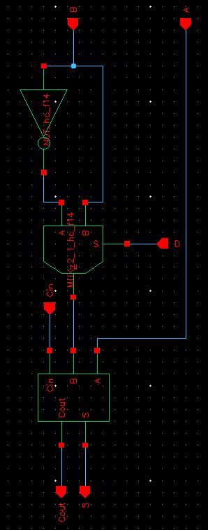
This circuit will provide A+B functionality when D=0 and A-B functionality when D=1.
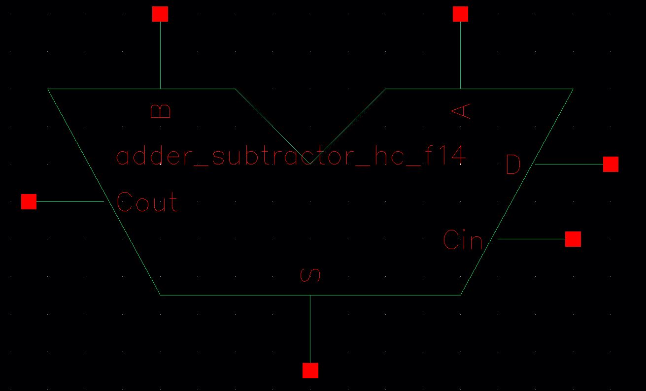
The symbol for this circuit is seen below.
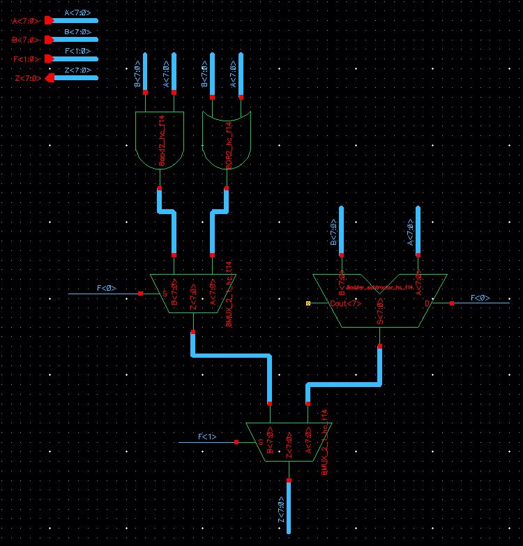
Next, it becomes necessary to create an 8-bit version of this adder/subtractor. Using a concise method of naming instances, the following schematic was created to represent the 8-bit version of the adder/subtractor.
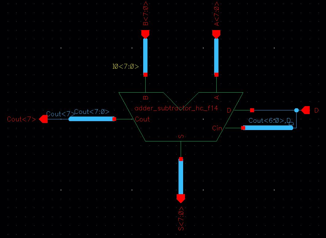
Notice the single wire for all D inputs, however only the first instance I0 will use D for Cin. The other instances will use their previous neighbor's Cout values for Cin.
After the adder/subtractor is made, the ALU is now formed.
The ALU follows the operations:
| F0 | F1 | Operation |
| 0 | 0 | AND |
| 0 | 1 | OR |
| 1 | 0 | A+B |
| 1 | 1 | A-B |
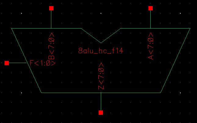
A symbol is then created for simulation purposes.
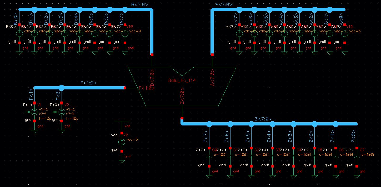
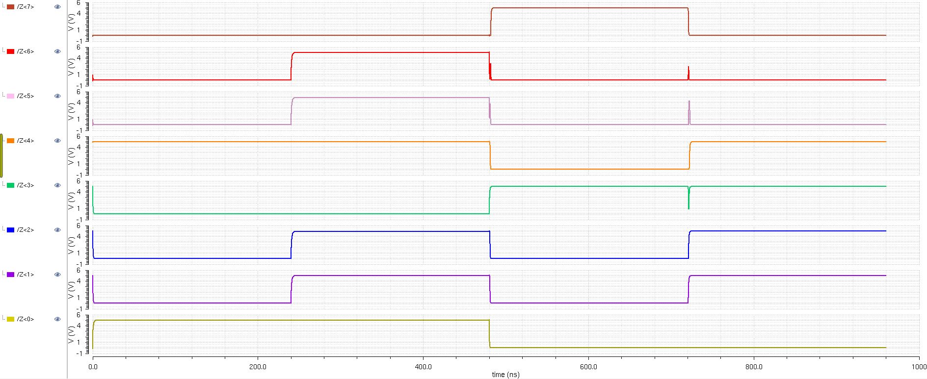
In order to verify the function of the ALU, a simulation schematic was setup.
The results are as follows:
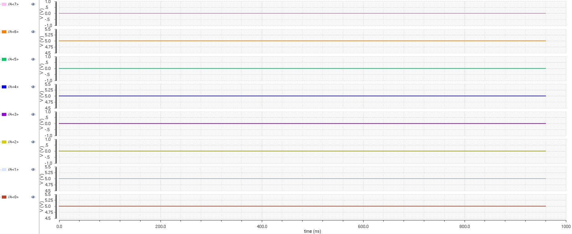
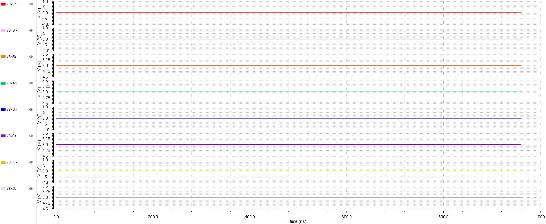
| 7 | 6 | 5 | 4 | 3 | 2 | 1 | 0 | Decimal | |
| A | 0 | 1 | 0 | 1 | 0 | 0 | 1 | 1 | 83 |
| B | 0 | 0 | 1 | 1 | 0 | 1 | 0 | 1 | 53 |
| Z | |||||||||
| F=00, AND | 0 | 0 | 0 | 1 | 0 | 0 | 0 | 1 | |
| F=01, OR | 0 | 1 | 1 | 1 | 0 | 1 | 1 | 1 | |
| F=10, A+B | 1 | 0 | 0 | 0 | 1 | 0 | 0 | 0 | 136 |
| F=11, A-B | 0 | 0 | 0 | 1 | 1 | 1 | 1 | 0 | 30 |
Simulation Plot:
F inputs: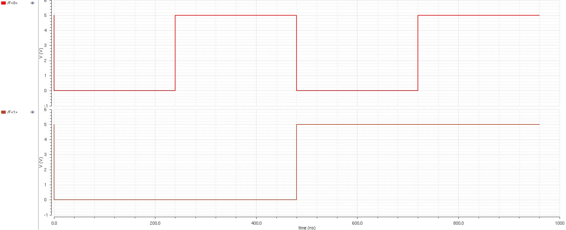
A inputs:
B inputs:
Z outputs:
This concludes Part I of the project. Files can be found here. Remember, some parts of the project are dependent on previous labs and it is important to include those parts when dealing with this project.
Part II - Layouts
This part of the project involves laying out the ALU.
There are multiple components that will be layed out individually, then combined to create the layout of the ALU.
The components that will be layed out individually are:
- 8-bit AND
- 8-bit OR
- 8-bit MUX
- 8-bit adder/subtractor
8-bit AND
We create the layout of the 8-bit AND gate by creating the individual AND gate layout. This individual AND gate layout was created by combining a NAND layout with an inverter layout.
This individual layout was instantiated 8 times to form the 8-bit AND layout.
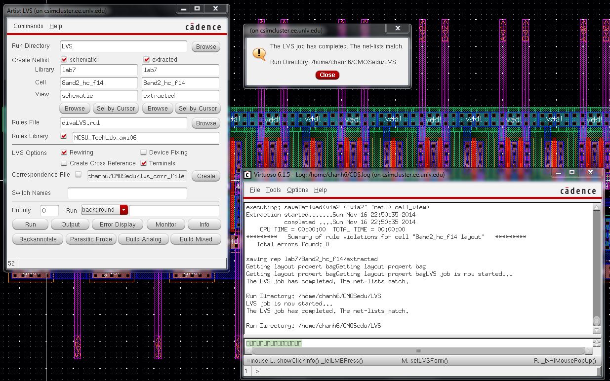
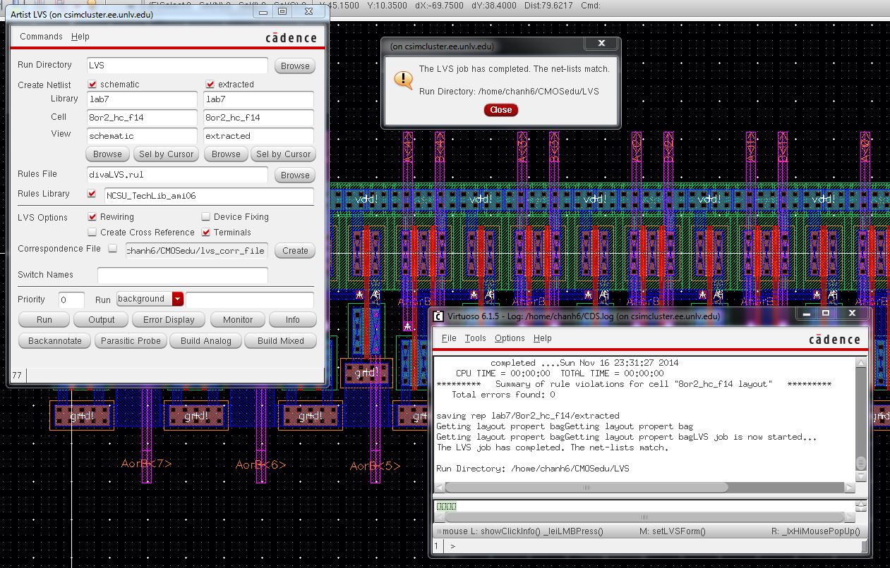
The layout DRCs and LVSs!
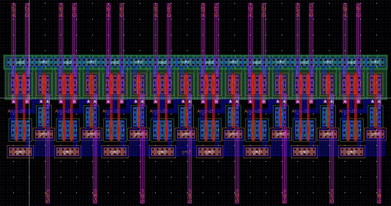
8-bit OR
We create the layout of the 8-bit OR gate by creating the individual OR gate layout. This individual OR gate layout was created by combining a NOR layout with an inverter layout.
This individual layout was instantiated 8 times to form the 8-bit OR layout.
The layout DRCs and LVSs!
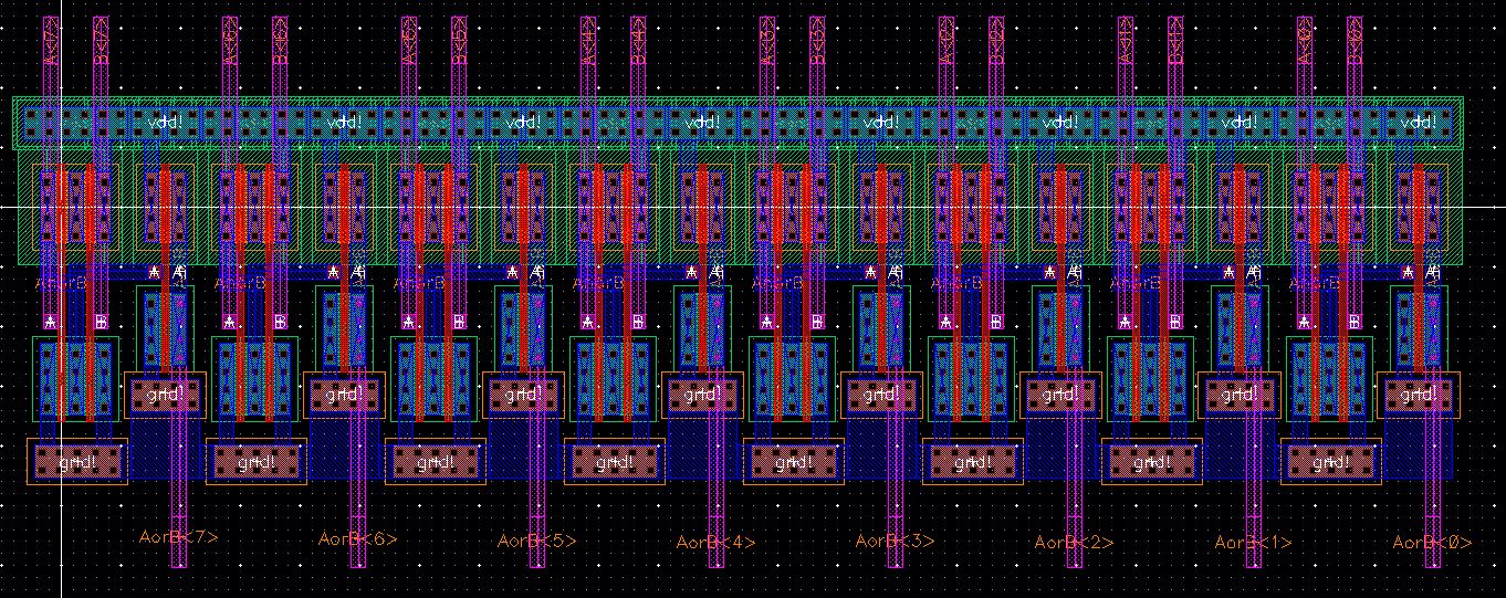
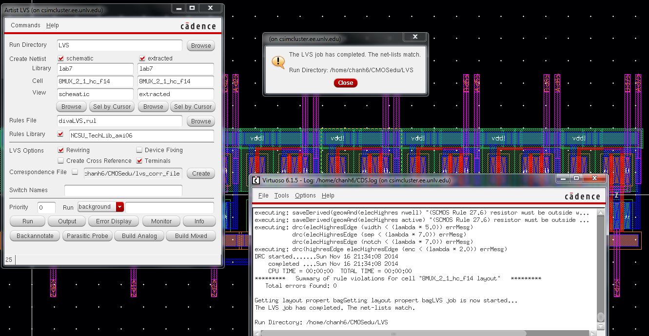
8-bit MUX
We create the layout of the 8-bit MUX by creating the individual MUX layout.
This individual layout was instantiated 8 times to form the 8-bit MUX layout. Connections are then formed that are consistent with the design. Notice that S connects to each individual MUX such that the 8-bit MUX will select the same input pin (A or B) for every individual MUX.
The layout DRCs and LVSs!
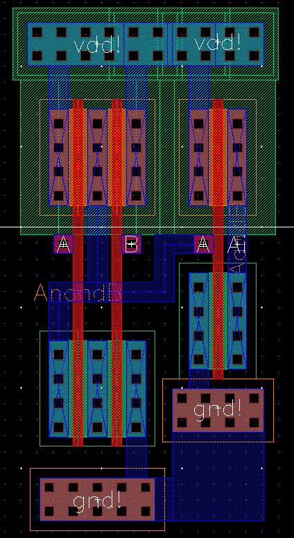
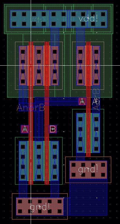
8-bit Adder/Subtractor
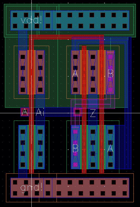
We create the 8-bit Adder/Subtractor based on the schematic in Part I. We start by putting the inverter and MUX together.
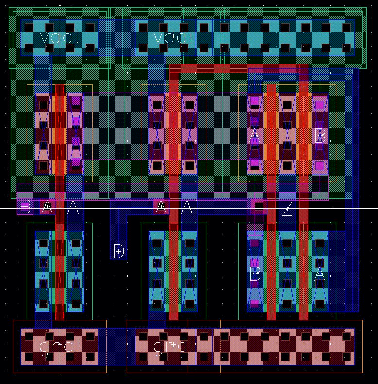
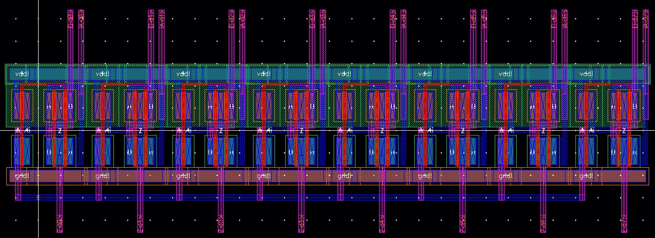
8 instances of this are used along with the previously created 8-bit fulladder/subtractor layout from lab 7.
fulladder layout:
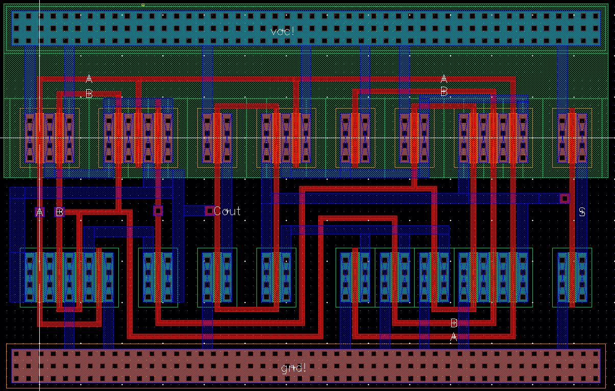
8-bit fulladder:
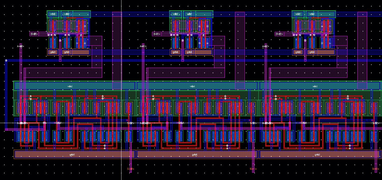
8-bit fulladder/subtractor (inverter+mux+fulladder):
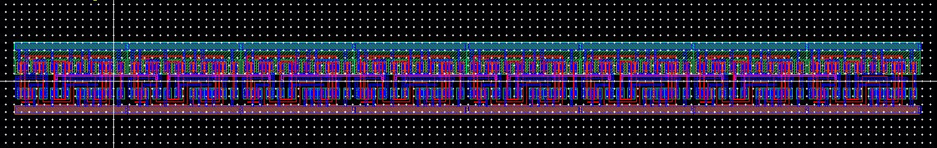
Left view (closeup):
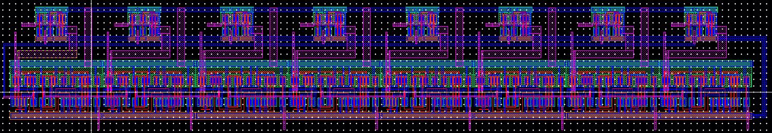
Right view (closeup):
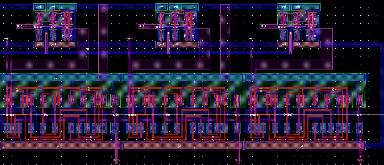
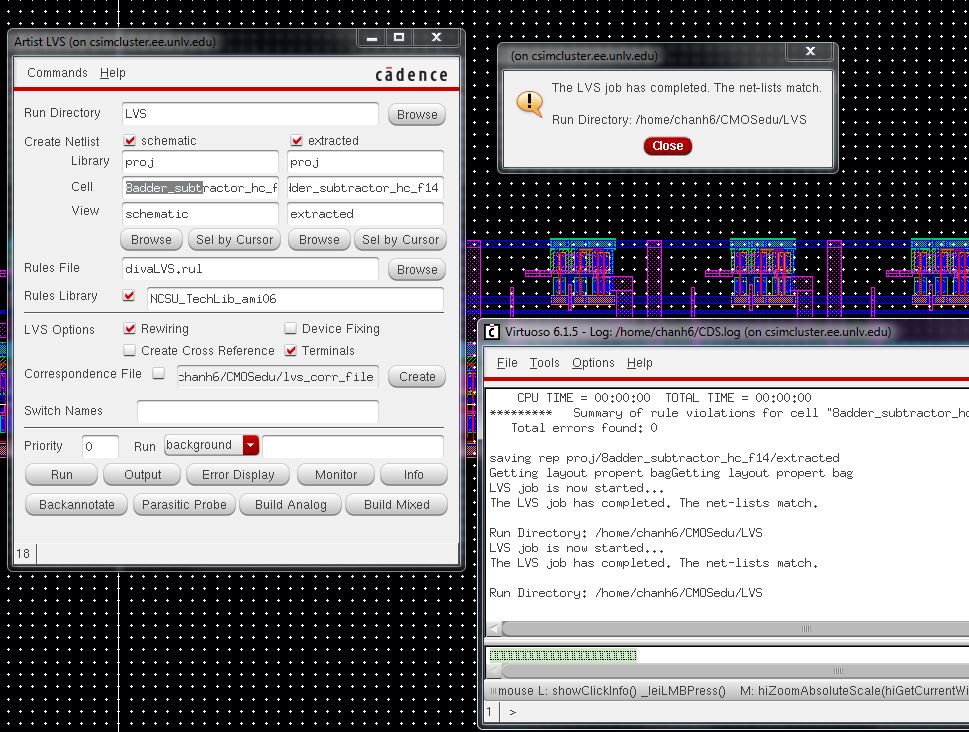
It LVSs and DRCs!
Now we can begin to create the ALU!
8-bit ALU
By combining all the previous layouts, we end up with the following:
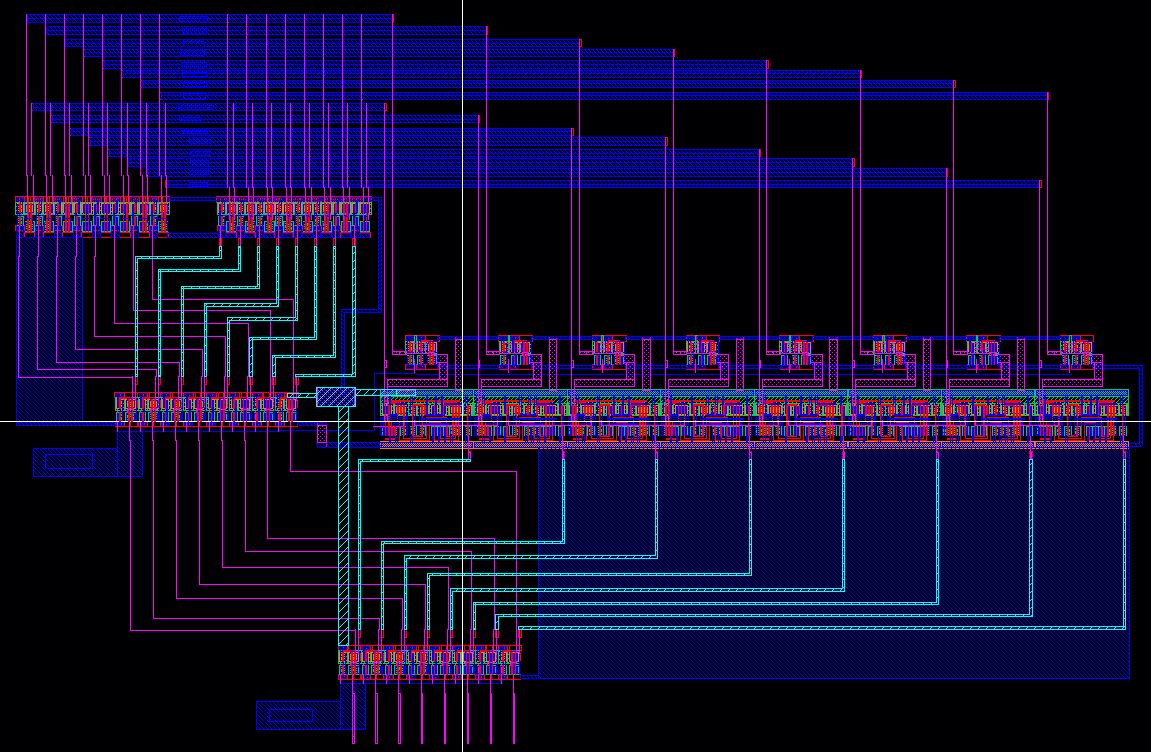
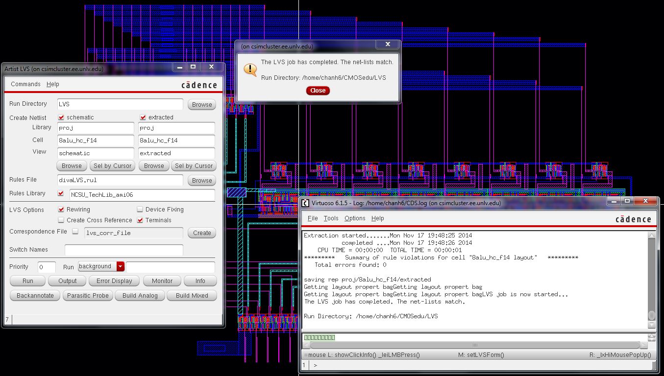
Finally, the layout DRC and LVS checks out!
All parts of this project were created using components from two libraries: lab7 and proj
*** IT IS IMPORTANT TO INCLUDE BOTH LIBRARIES IN ORDER TO EXAMINE THE DESIGN ***
Backups were made using a cloud storage method.