Lab 7 - EE 421L
Authored
by Henry Chan,
chanh6@unlv.nevada.edu
October 27, 2014
Using buses and arrays in the design of word inverters, muxes, and high-speed adders
Examining a 4-bit word inverter
The inverter uses 6u/0.6u NMOS and PMOS devices.
Using separate instances for each inverter is viable.
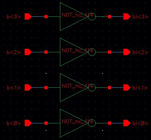
In
large circuits with large numbers of instances, using individual
instances similar to above becomes cluttered. A better method for more
compact and concise schematics is shown below:
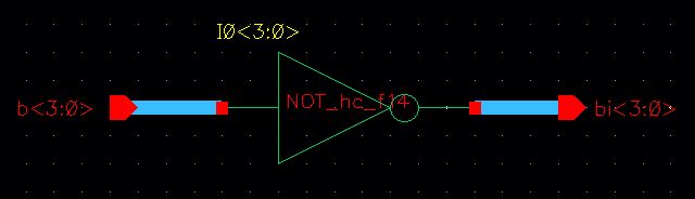
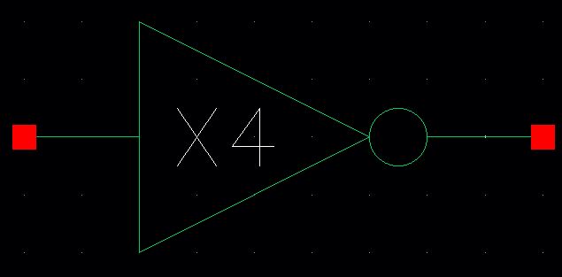
A symbol was created using the concise schematic.
This symbol was then used in a simulation schematic to determine correct functionality.
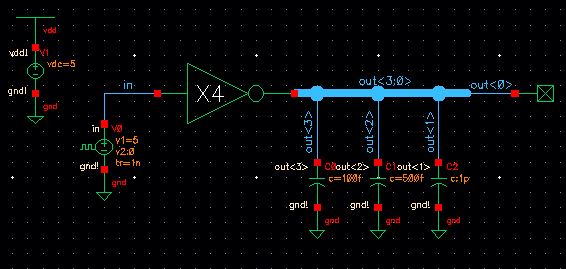
Below are the results:
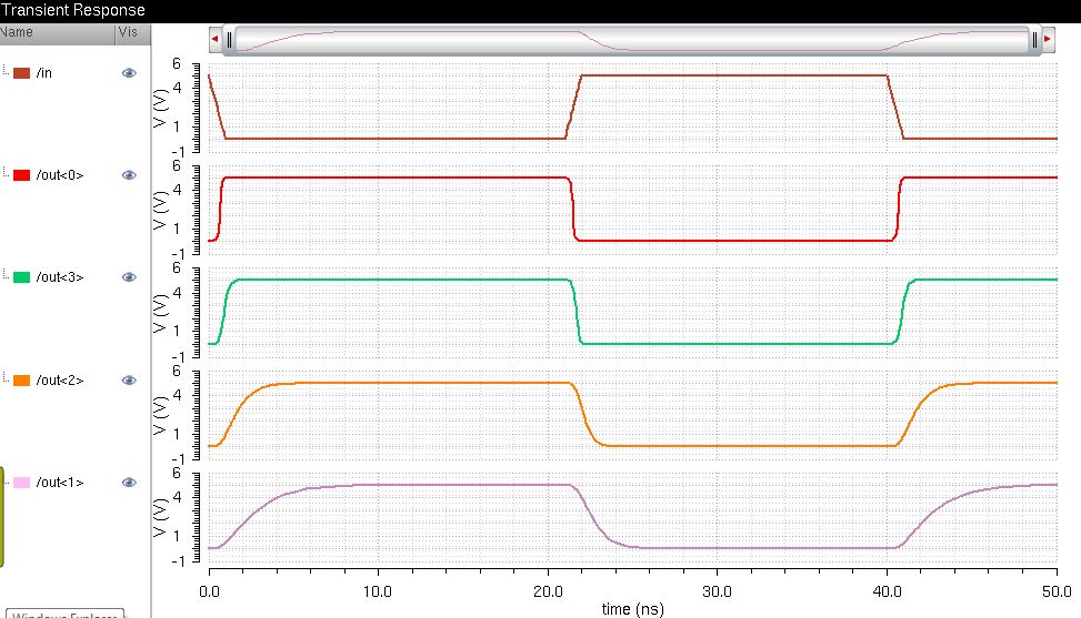
As
you can see, the greater the capacitive load, the greater the delay to
the output. out0 demonstrates the resulting signal with no load
attached. out3 hosts a 100fF load, out2 a 500f load, and out1 a 1pF
load. As the loads increase, the outputs generally become more delayed
and exhibit larger rise and fall times.
Now
that we have examined a concise method for creating multiple instances,
we will begin creating logic gates that utilize this method to form an
8-bit word full-addder. This will include an inverter, nand gates, nor
gates, and gates, and or gates.
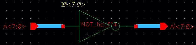
8-bit Inverter
Schematic
Symbol
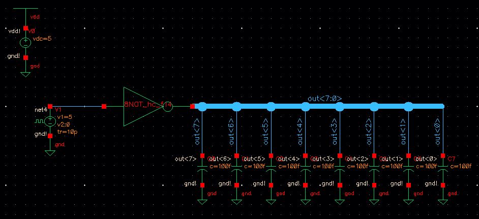
Simulation Schematic
Simulation Plot
Because
I am applying the same signal to all 8 inputs, the outputs are bound to
be the same, thus overlapping each other in the plot.
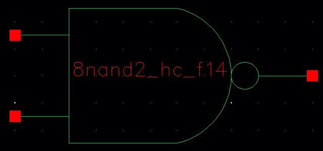
8-bit NAND Gate
In order to create an 8-bit NAND, I first create the 1-bit NAND gate:
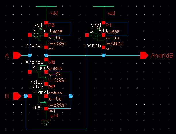
1-bit NAND Gate Schematic
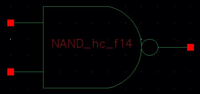
1-bit NAND Gate Symbol
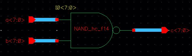
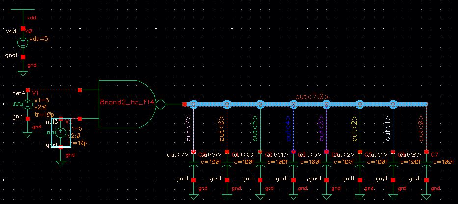
Using this 1-bit NAND symbol, I create the 8-bit NAND Gate using the concise method.
8-bit NAND Gate Schematic
8-bit NAND Gate symbol
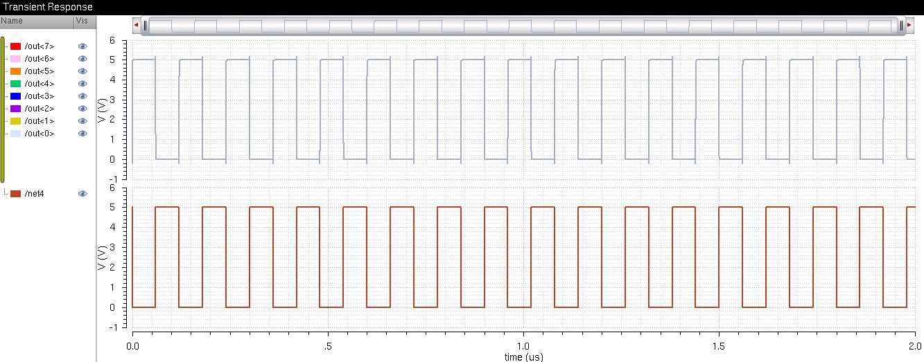
8-bit NAND Simulation Schematic
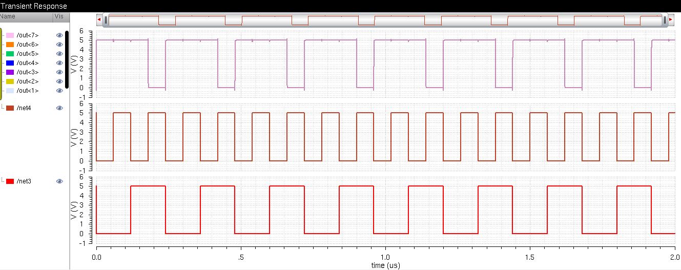
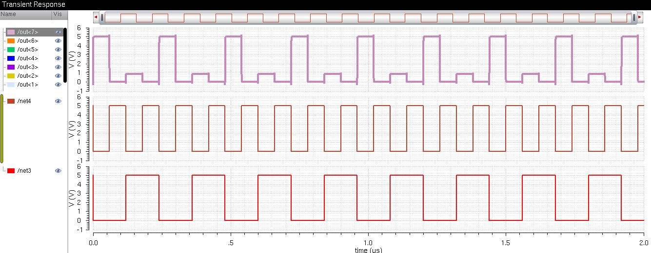
8-bit NAND Simulation Plot
Net3 represents B and Net4 represents A, the output folllows the following table:
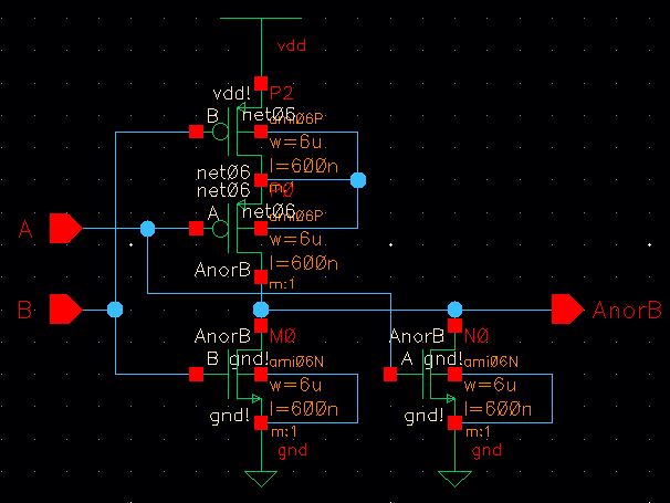
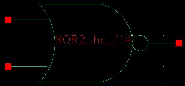
8-bit NOR Gate
1-bit NOR Schematic
Similar to the 8-bit NAND, I have to create the 1-bit NOR in order to create the 8-bit NOR.
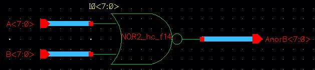
1-bit NOR Symbol
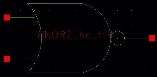
8-bit NOR Schematic
8-bit NOR Symbol
8-bit NOR Simulation Schematic
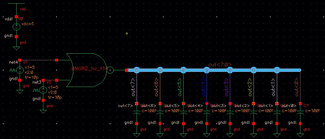
8-bit NOR Simulation Plot
The NOR output follows the following table:
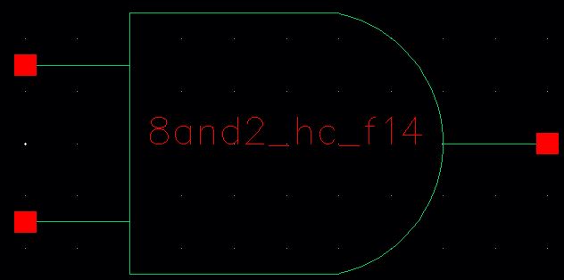
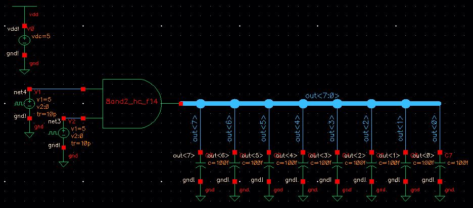
8-Bit AND Gate
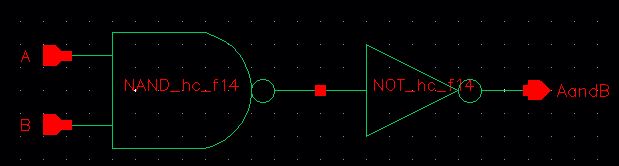
I created the AND gate by simply using the NAND symbol and an inverter.
1-bit AND Schematic
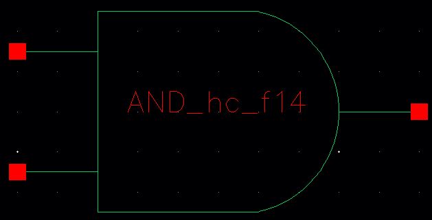
1-bit AND Symbol
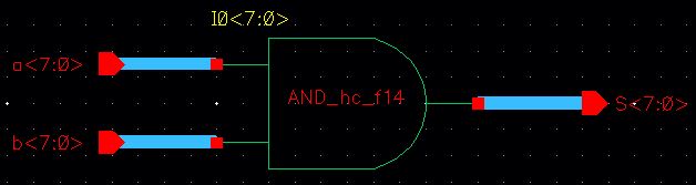
8-bit AND Schematic
8-bit AND Symbol
8-bit AND Simulation Schematic
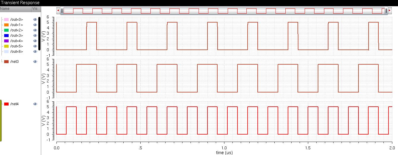
8-bit AND Simulation Plot
The output follows the following table:
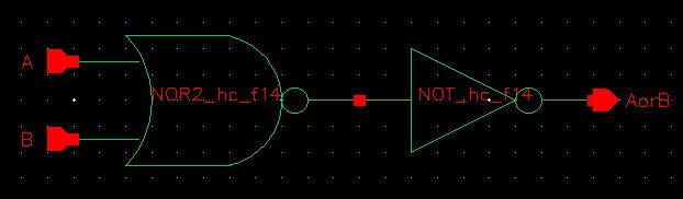
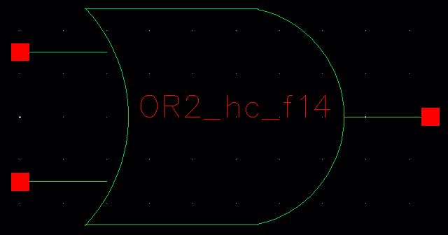
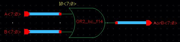
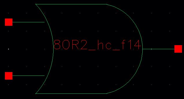
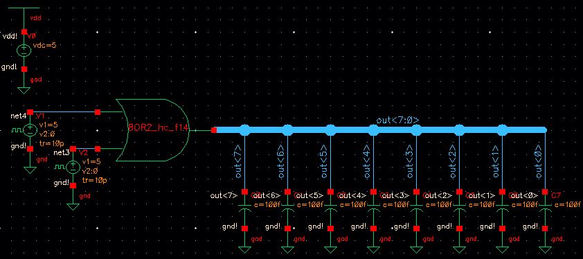
8-bit OR Gate
1-bit OR Schematic
I used the NOR gate and an inverter to make the OR gate.
1-bit OR Symbol
8-bit OR Schematic
8-bit OR Symbol
8-bit OR Simulation Schematic
8-bit OR Simulation Plot
The output follows the following table:
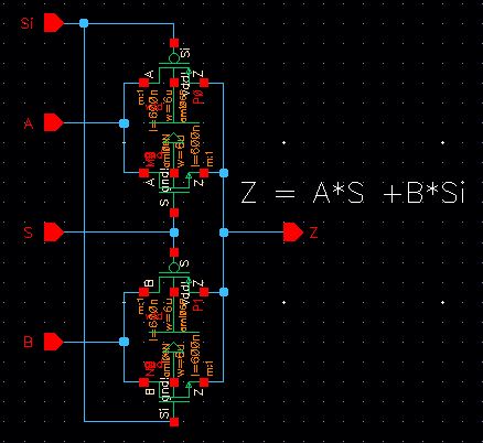
2-1 MUX
1-bit 2-to-1 MUX schematic
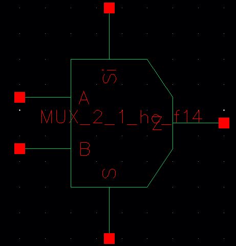
1-bit 2-to-1 MUX Symbol
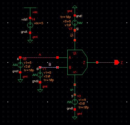
1-bit 2-to-1 MUX Simulation Schematic
1-bit 2-to-1 MUX Simulation Plot
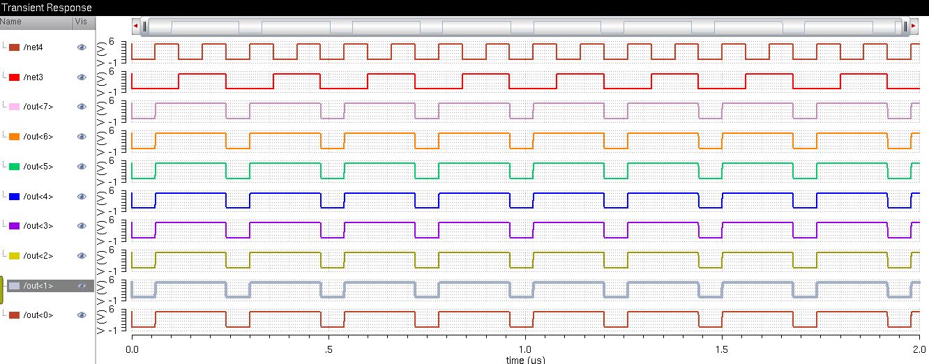
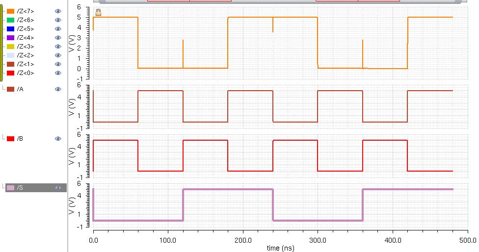
8-bit 2-to-1 MUX
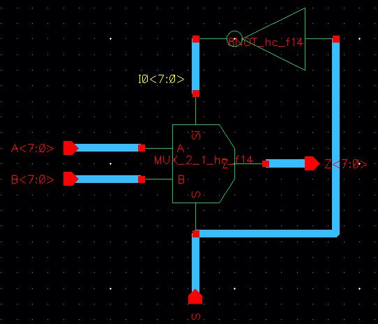
8-bit 2-to-1 MUX Schematic
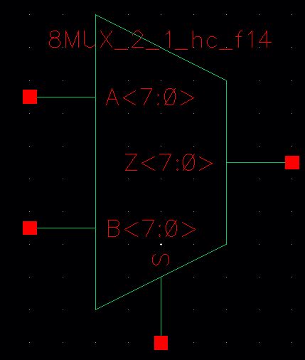
8-bit 2-to-1 MUX Symbol
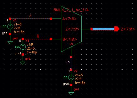
8-bit 2-to-1 Simulation Schematic
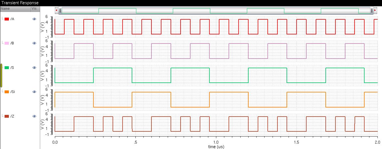
8-bit 2-to-1 Simulation Plot
When S is low, Z=B.
When S is high, Z=A.
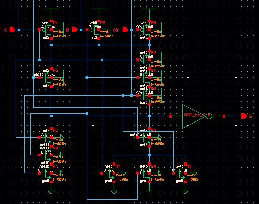
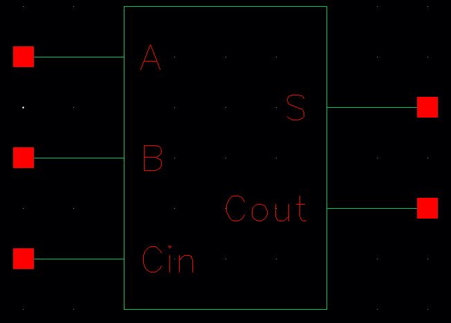
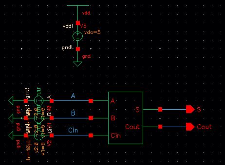
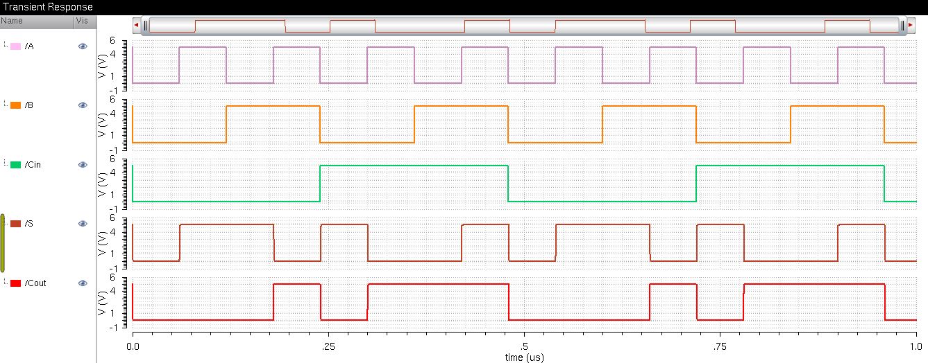
1-bit FULL ADDER
Schematic
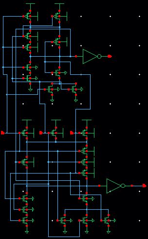
top:
bottom:
Symbol
Simulation Schematic
Simulation Plot
| Cin | B | A | S | Cout |
| 0 | 0 | 0 | 0 | 0 |
| 0 | 0 | 1 | 1 | 0 |
| 0 | 1 | 0 | 1 | 0 |
| 0 | 1 | 1 | 0 | 1 |
| 1 | 0 | 0 | 1 | 0 |
| 1 | 0 | 1 | 0 | 1 |
| 1 | 1 | 0 | 0 | 1 |
| 1 | 1 | 1 | 1 | 1 |
Layout
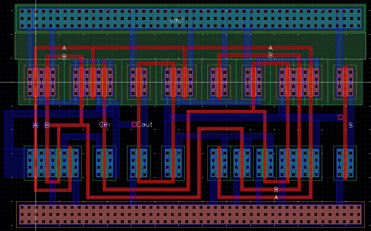
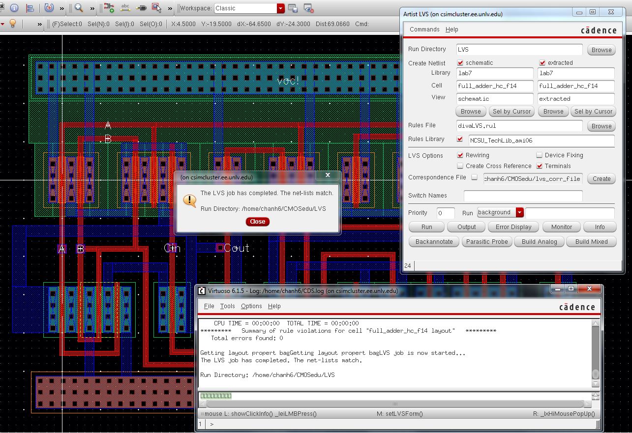
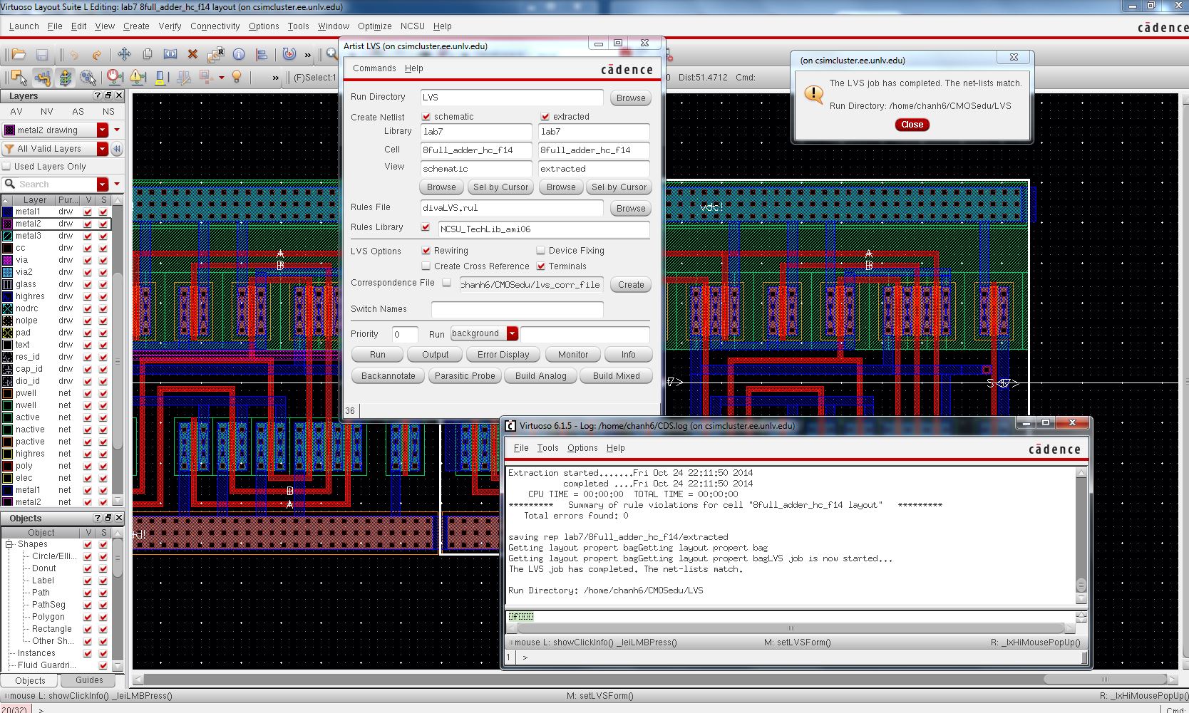
DRC and LVS
Everything checks out!
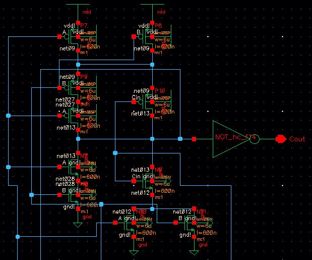
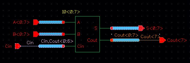
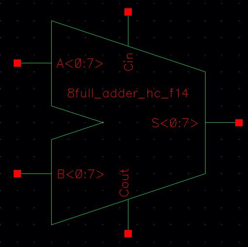
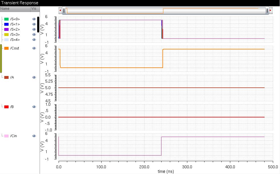
8-bit FULL ADDER
Schematic
Symbol
Simulation Schematic
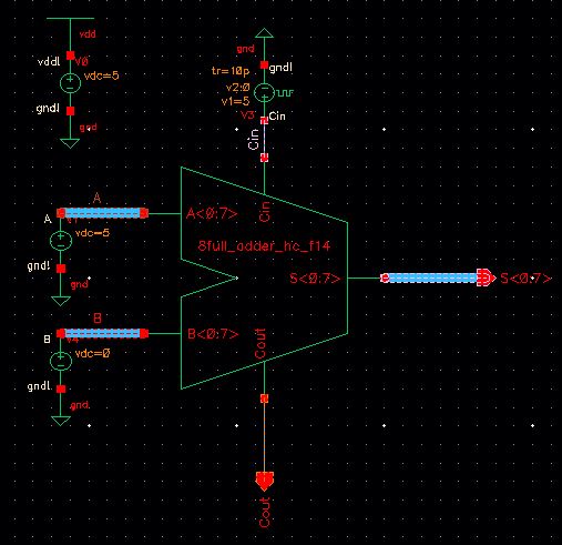
Notice, A is 1111,1111 and B is 0000,0000. Cin will alternate from 0 to 1.
Simulation Plot
S=1111,1111 and Cout=0 when Cin is 0 because A(1111,1111)+B(0000,0000)+Cin(0)=S(1111,1111), Cout(0)
S=0000,0000 and Cout=1 when Cin is 1 because A(1111,1111)+B(0000,0000)+Cin(1)=S(0000,0000), Cout(1)
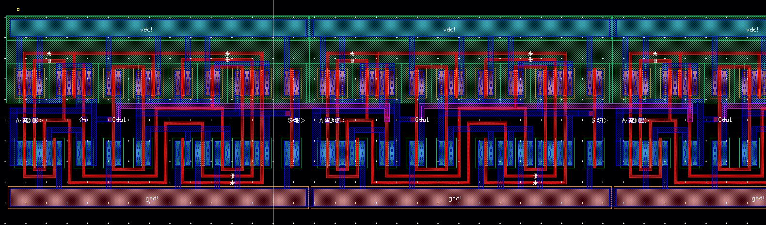
Layout
Using the 1-bit Full Adder Layout, I created multiple instances and connected them together.
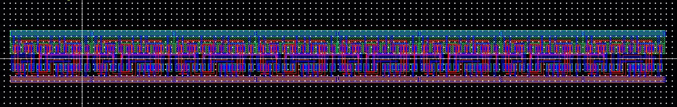
Left
Right
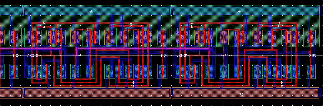
DRC and LVS
Everything checks out!
This ends the lab, all materials can be found here: lab7.zip
Backups were made using a cloud storage method.
Return to EE 421 Labs