Lab 5 - EE 421L
A symbol may be created from the cellview by clicking Create->Cellview->From Cellview
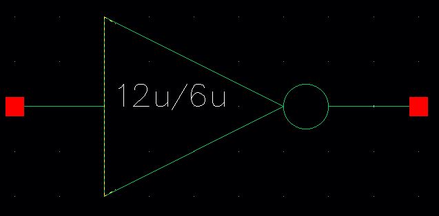
Deleting everything except for the pins allows us to draw the following symbol.
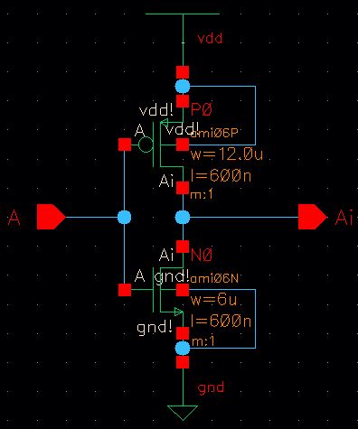
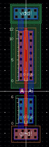
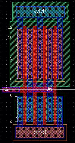
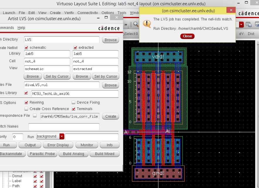
After the schematic and symbol are made, the layout may be produced.. Instances from the NCSU_TechLib_ami06 library were used to create the nmos and pmos layouts along with ntap and ptap instances. Width and length were adjusted accordingly and metal layers were connected to create the following.
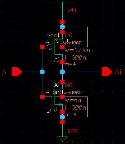
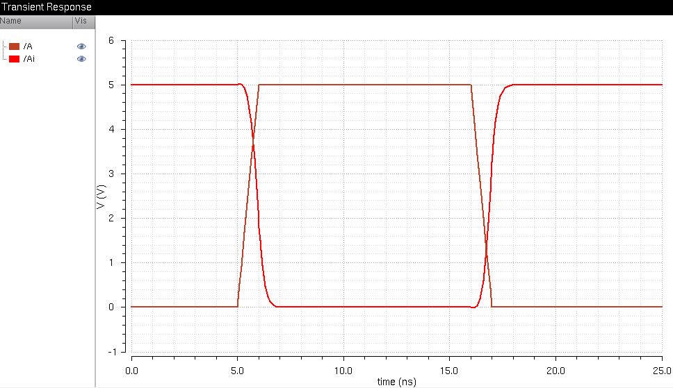
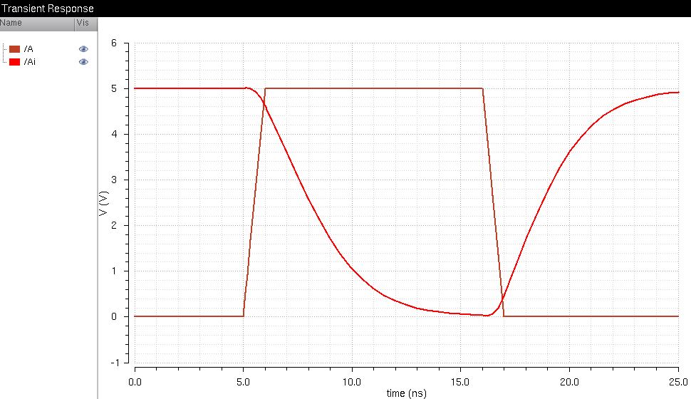
A represents the input and Ai represents the output
The power is run on the top of the cell using metal1 and ground is run on the bottom of the cell using metal1 as well.
Power (vdd!) is connected to the n-well using the ntap cell.
Ground (gnd!) is connected to the p-substrate using the ptap cell.
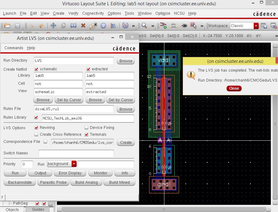
The layout LVS checks out.
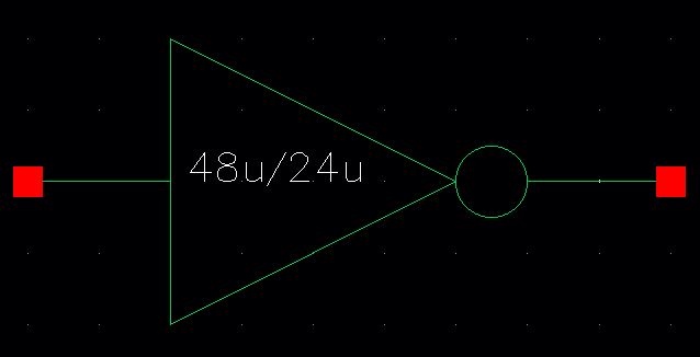
48u/24u Inverter
I copied the previous schematic to another cell view called not4 and used it as a template to produce the 48u/24u inverter. Simply by editing the properties of the transistors ('Q') and modifying the multiplier to 4, the 48u/24u inverter was created.
Using the same method as before, a successful symbol was created for the 48u/24u inverter.
The layout was then produced with the appropriate nmos and pmos characteristics from the NCSU_Techlib_ami06 library. Ntap, ptap, and metal1 connections were added to produce the 48u/24u inverter.
LVS was completed successfully.
Now that the components are created, it is time to simulate the devices.
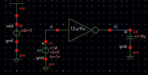

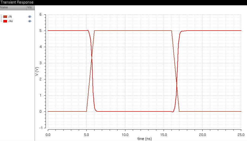
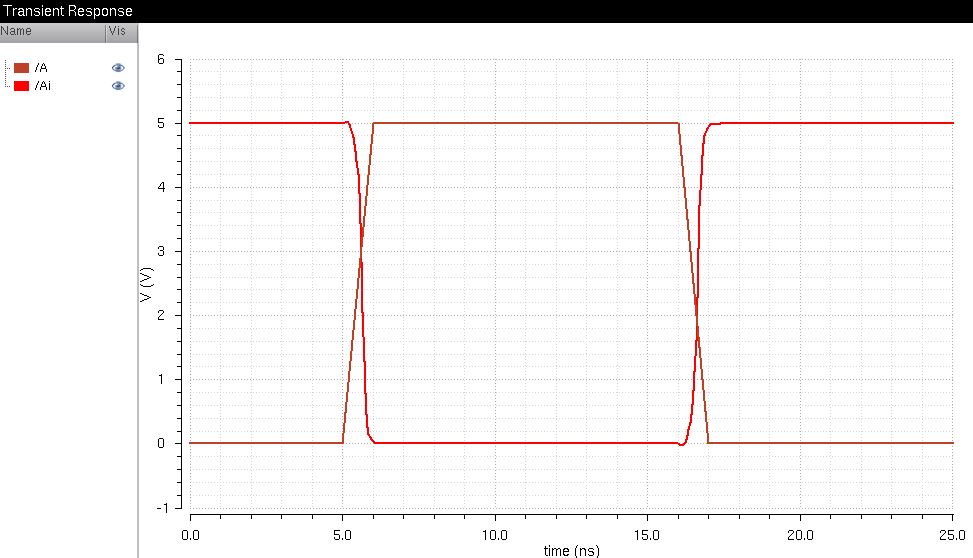
12u/6u Inverter - 1pF Capacitive Load
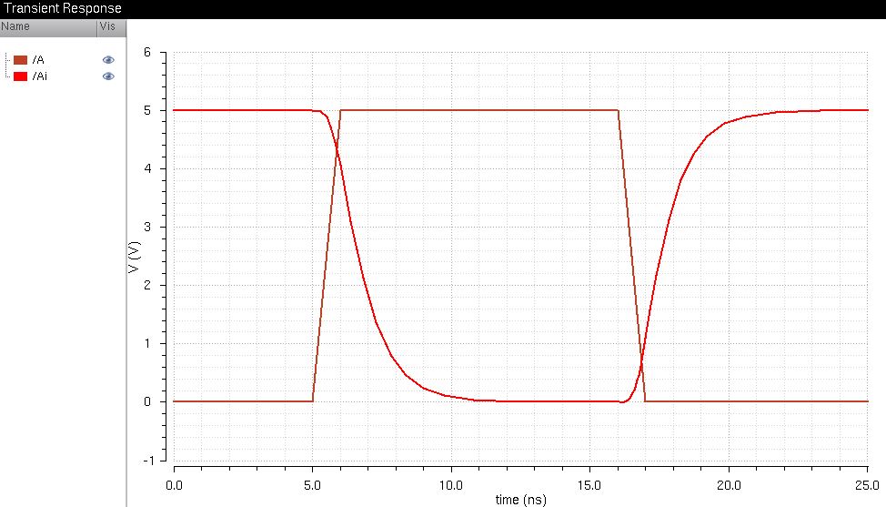
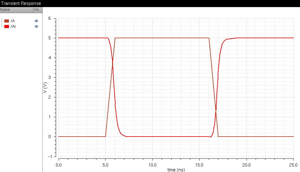
12u/6u Inverter - 10pF Capacitive Load

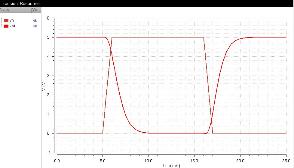
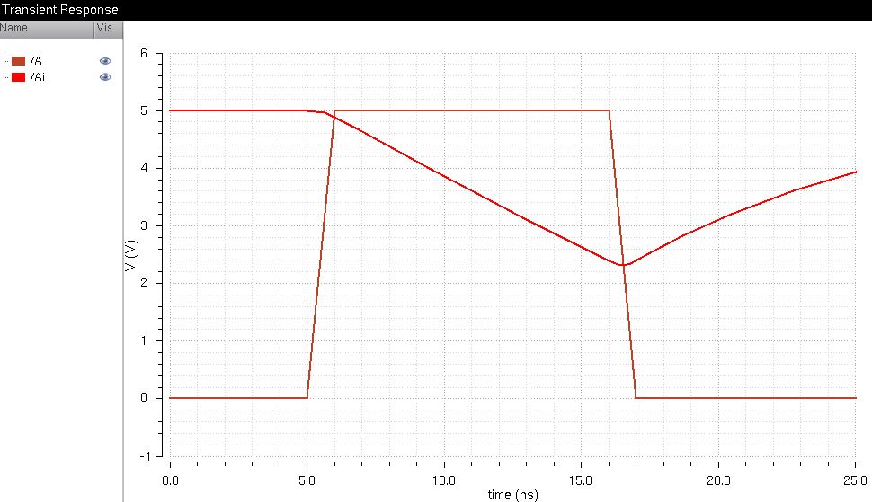
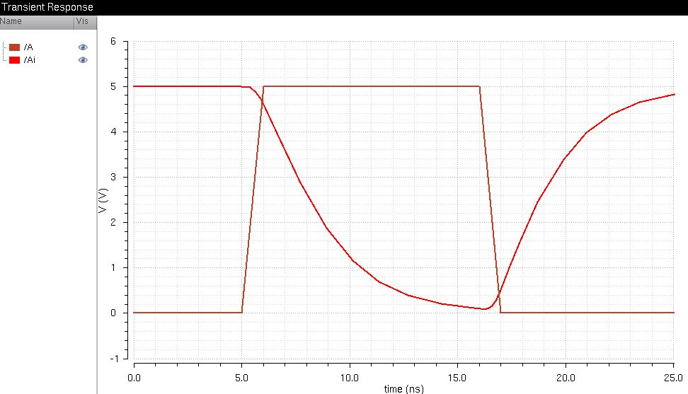
12u/6u Inverter - 100pF Capacitive Load
The simulation results are very telling when increasing the capacitive load to the inverter. As you raise the capacitance, the output begins tobehave less like an inverter and seems increasingly unresponsive to the input voltage.
48u/24u Simulations
Now that we've examined the 12u/6u inverter, it is time to examine the 48u/24u inverter.
The simulation schematic was easily created by copying the 12u/6u schematic and simply changing the inverter to the 48u/24u inverter.
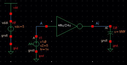
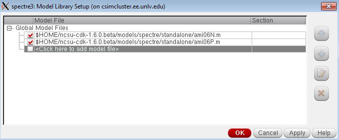
Opening the ADE window again will allow us to produce the simulations. (Don't forget to include the model libraries!)
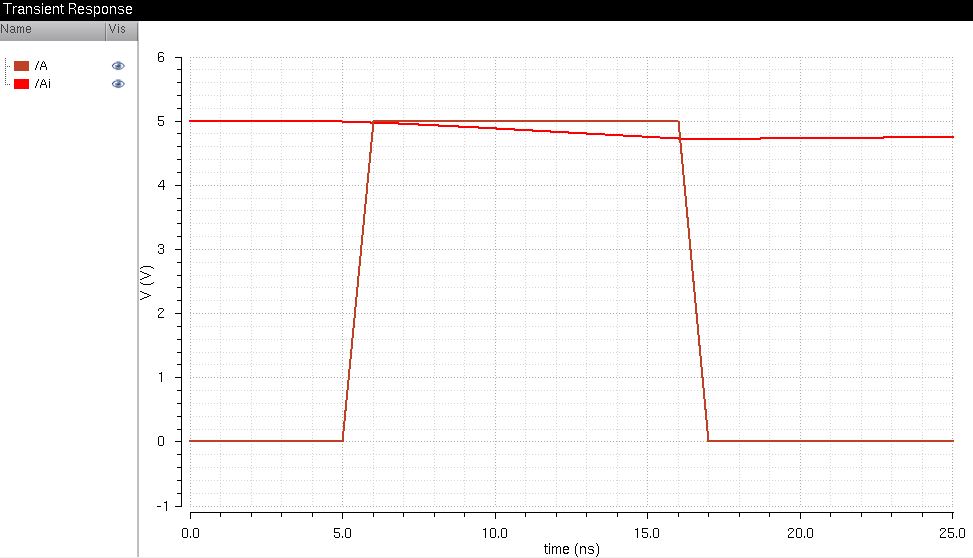
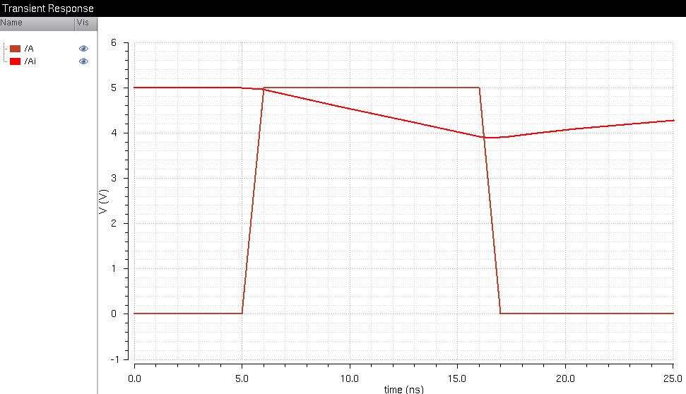
48u/24u Inverter - 100fF Capacitive Load
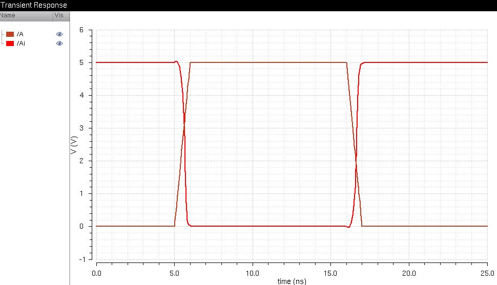
48u/24u Inverter - 1pF Capacitive Load
48u/24u Inverter - 10pF Capacitive Load
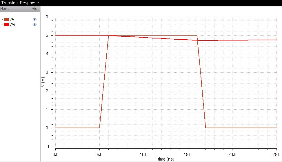
48u/24u Inverter - 100pF Capacitive Load

As you can see, the 48u/24u while still suffering from unresponsiveness, still performs slightly better than its 12u/6u counterpart.
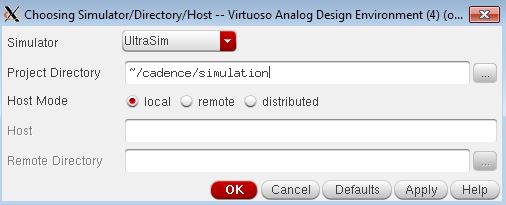
Up to this point, all simulations have been run using spectre, however, sometimes it is appropriate to use UltraSim, a faster, but less accurate simulator found. (UltraSim is typically used for larger circuits for its fast simulation times)
It is also important to note that UltraSim only performs transient simulations.With the ADE window selected, click Setup -> Simulator/Directory/Host -> and select UltraSim similar to the image below.
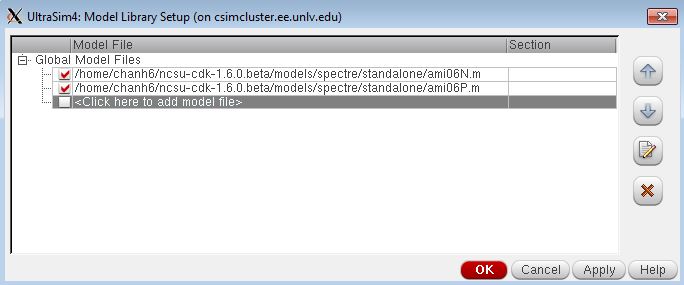
(Don't forget to setup the model libraries!)
12u/6u Inverter - 100fF Capacitive Load (UltraSim)
12u/6u Inverter - 1pF Capacitive Load (UltraSim)
12u/6u Inverter - 10pF Capacitive Load (UltraSim)
12u/6u Inverter - 100pF Capacitive Load (UltraSim)
48u/24u Inverter - 100fF Capacitive Load (UltraSim)
48u/24u Inverter - 1pF Capacitive Load (UltraSim)
48u/24u Inverter - 10pF Capacitive Load (UltraSim)
48u/24u Inverter - 100pF Capacitive Load (UltraSim)
End of Lab 5
Files from this lab may be found here.
Backups were made using cloud storage.