Lab 4 - EE 421L
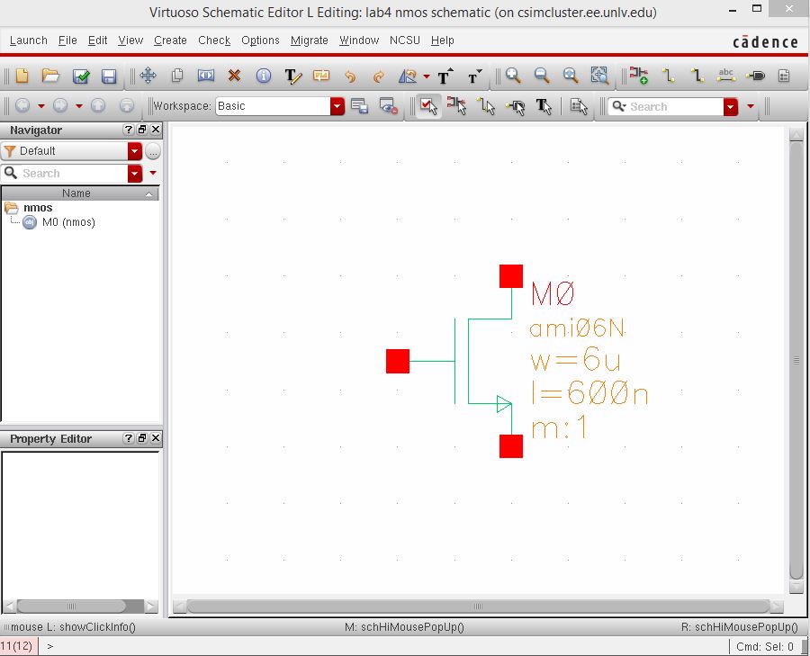
We end up with the below.
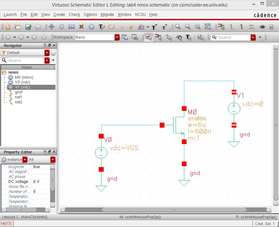
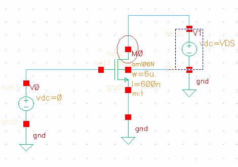
Using
two voltage sources, the schematic is setup to sweep the V1 voltage
source so that we sweep the voltage at the drain and source.
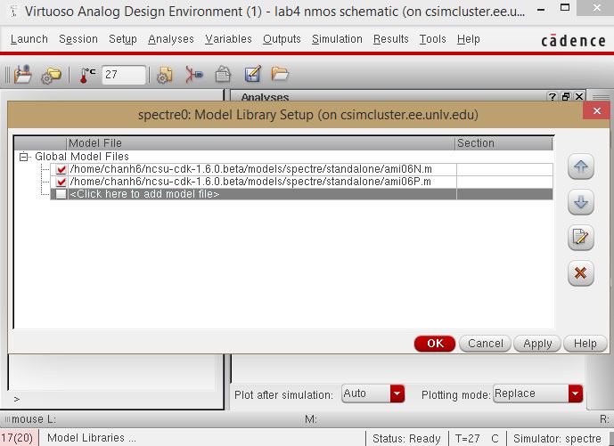
Now, we have some configuring to do, it is necessary to open the Analog Design Environment and clicking on SETUP->MODEL LIBRARIES
Make sure you include the model files shown below. These will make sure our simulation works as intended.
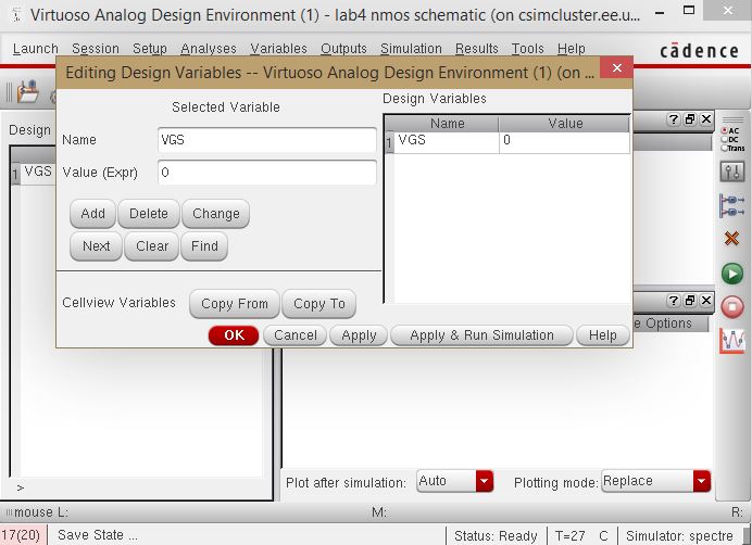
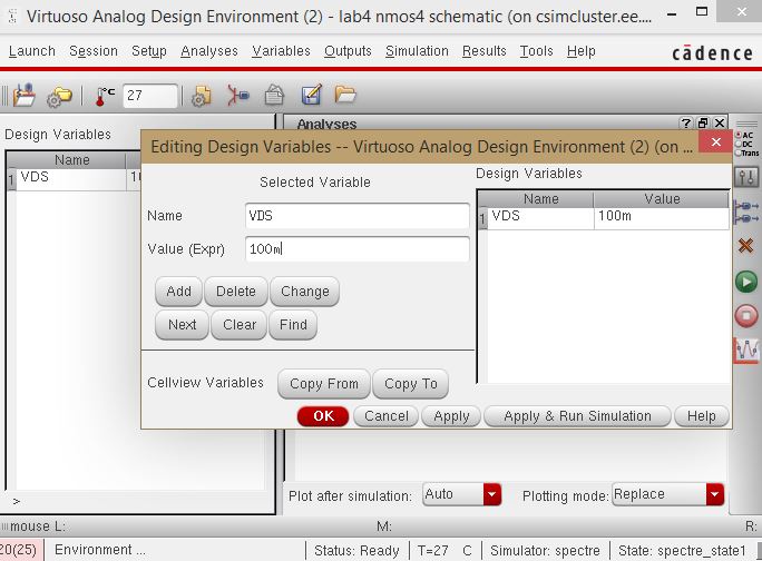
Next, variables are set up by clicking on Variables->EDIT
Set the VGS variable to 0.
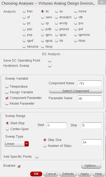
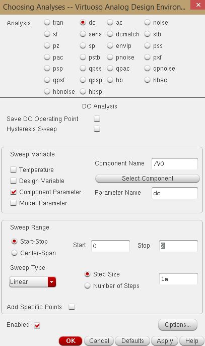
Now we choose the type of analysis. We will be choosing DC analysis to sweep our V1 voltage source from 0 to 5 in 1mV increments.
Choose the same parameters as the image below.
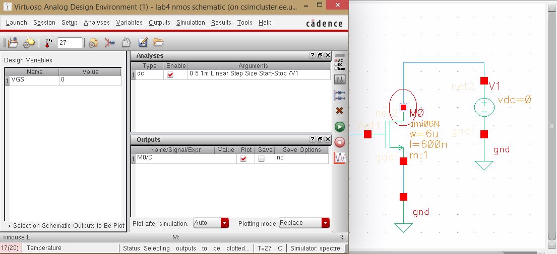
Make sure the output we are plotting is the current through the drain. You can do this by clicking on OUTPUTS->TO BE PLOTTED->SELECT ON SCHEMATIC.
Note the circle on the schematic indicates that we have selected it as an output.
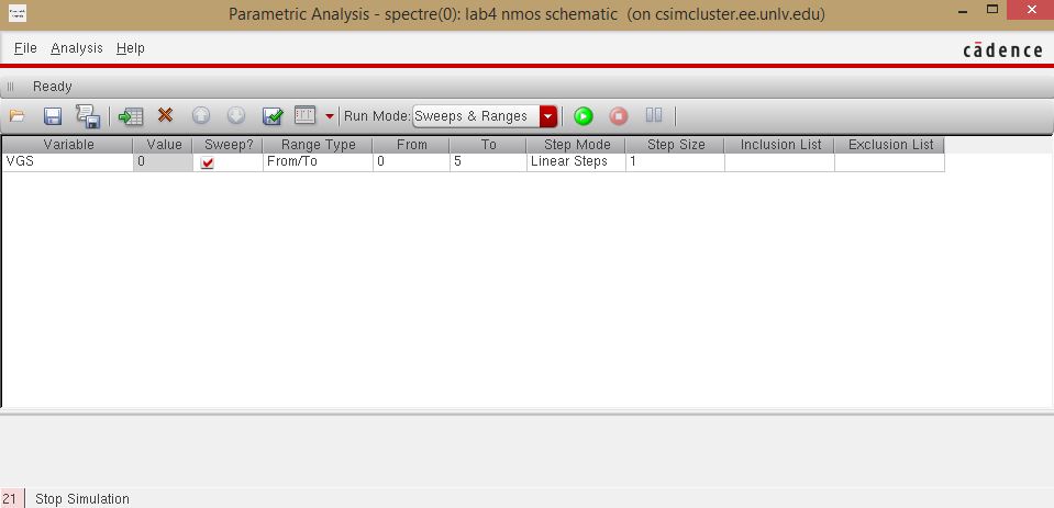
We want to see the effect of the VDS increments at different VGS voltages, therefore we will choose a Parametric Analysis.
This
will create different traces for each value of VGS we specify (in this
case we are examining VGS from values 0V to 5V with 1V steps).
Open ADE-L again to setup our simulation. The analysis window should look similar to below.
We
won't be using Parametric Analysis this time because we are only
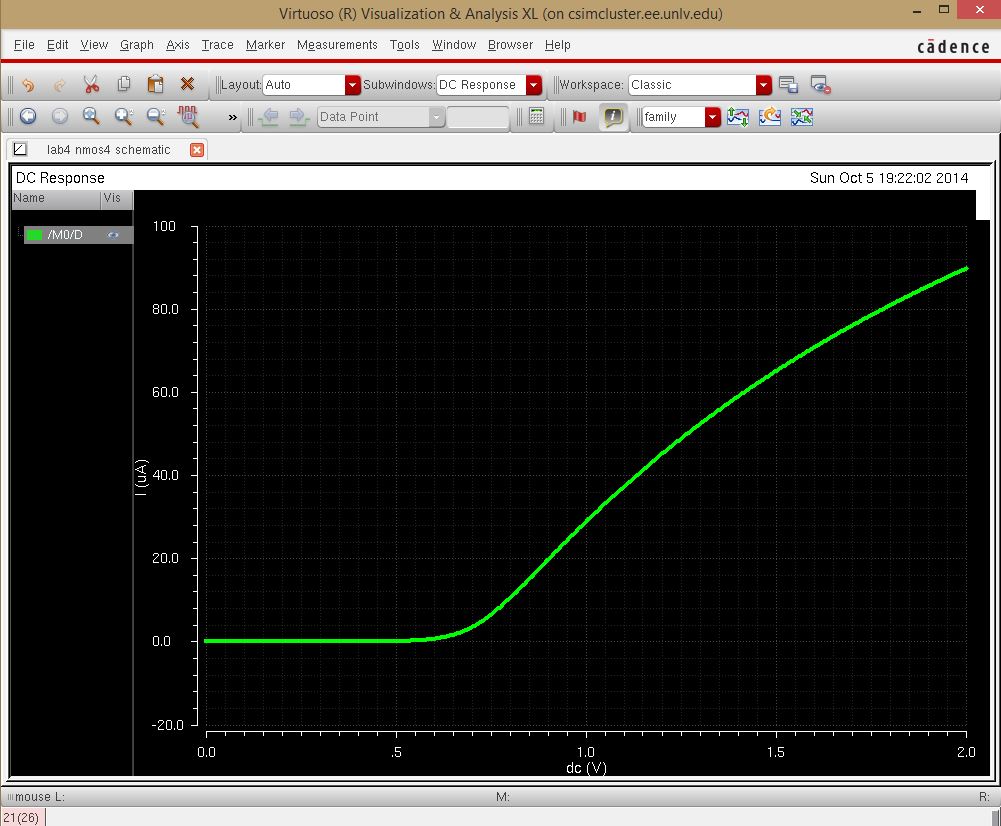
interested in sweeping the VGS at a single VDS voltage of 100mV.
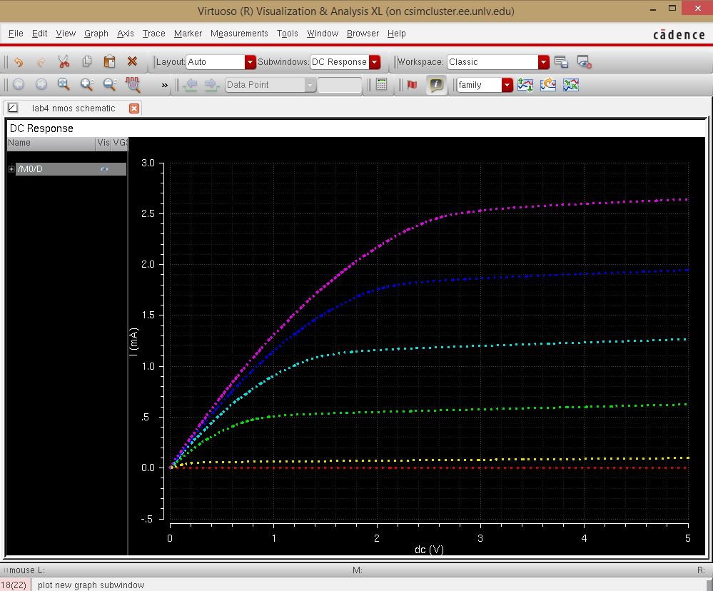
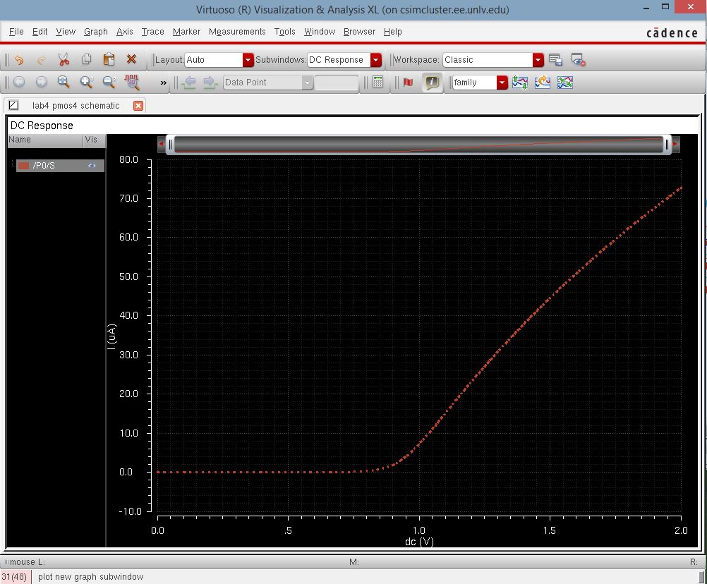
The results of the simulation appears as follows:
Now it is time to move on to PMOS!
PMOS
ID vs. VSD
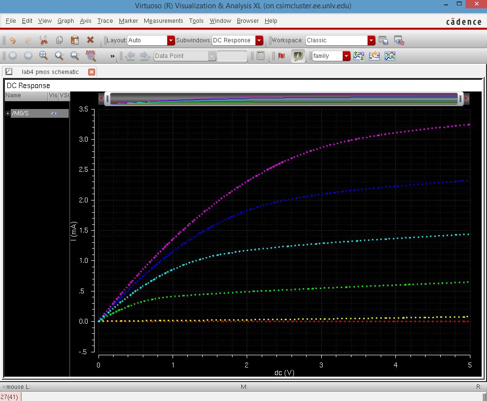
We will be simulating ID vs. VSD of a PMOS device for VSG varying from 0 to 5V in 1V steps while VSD varies from 0 to 5V in 1mV steps.
This will be using a width-to-length ratio of 12u/0.6u. It is important to make this adjustment in the schematic!
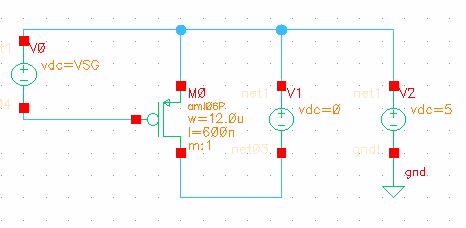
Begin by setting up a seperate schematic for the PMOS.
Your schematic should look like this:
We setup our analysis for our PMOS in the same way we setup our NMOS analysis, except we will be using different parameters.
Below, you can see the appropriate variables, analyses, outputs, and parametric analysis setups.
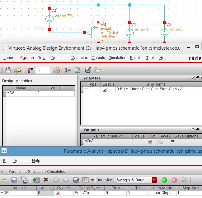
Clicking the green button will give us our results for the ID vs. VSD in a PMOS device.
ID vs. VSG
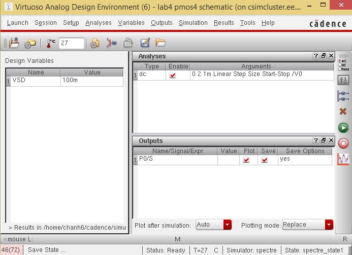
In this sim, we will be examining ID vs. VSG of a PMOS device for VSD = 100mV where VSG varies from 0 to 2V in 1mV steps.
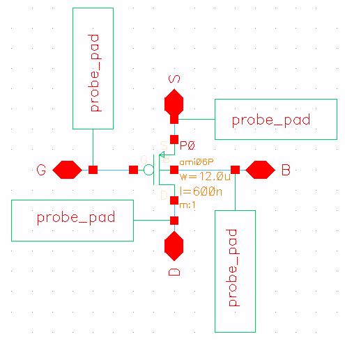
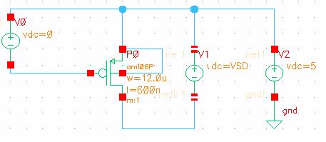
A 12u/0.6u width-to-length ratio will be used again, however, we will be using a four terminal PMOS in this simulation.
Make the necessary adjustments in the schematic to replace the pmos instance with a pmos4 instance.
Making the necessary adjustments again, this is what the analysis window should look like.
Click on the green run button to display the results of the simulation!
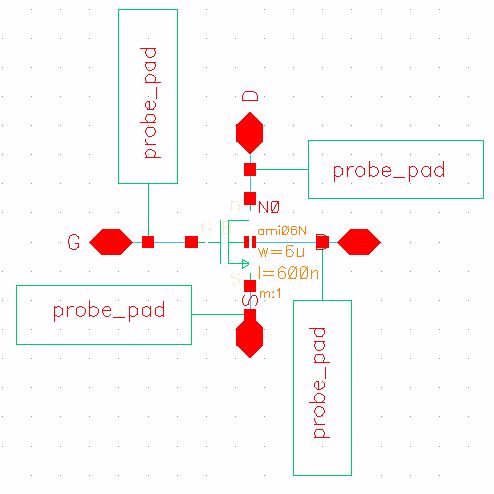
NMOS LAYOUT
It is now time to layout our four terminal NMOS device and attach it to probe pads.
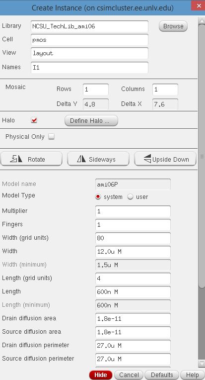
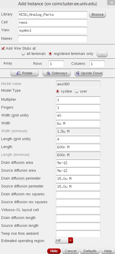
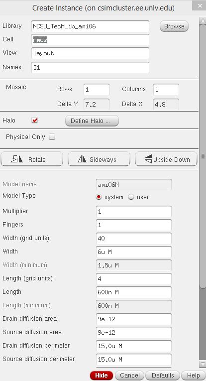
Create a new cell and a new layout in that cell. We will be laying out an NMOS with a 6u/0.6u width-to-length ratio.
Start by creating an instance of the nmos layout from the NCSU_TechLib_ami06 as seen below.
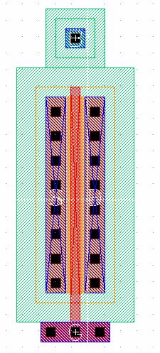
Then extend the poly slightly and add a m1_poly instance to form our gate.
Tie the p-substrate to ground by using a ptap instance and labeling it with a pin to ground.
Also, label the drain and source with pins as well.
Now this layout needs some probe pads to connect to.
Using m2_m1 connections and m3_m2 connections, we end up connecting the NMOS to probe pads as such:
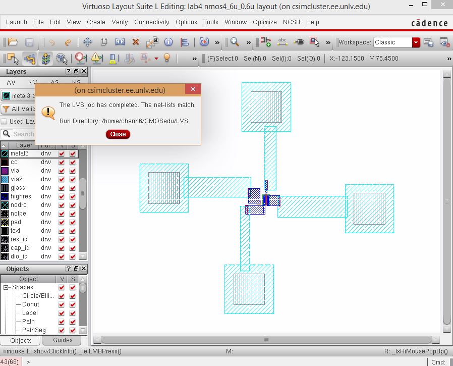
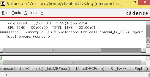
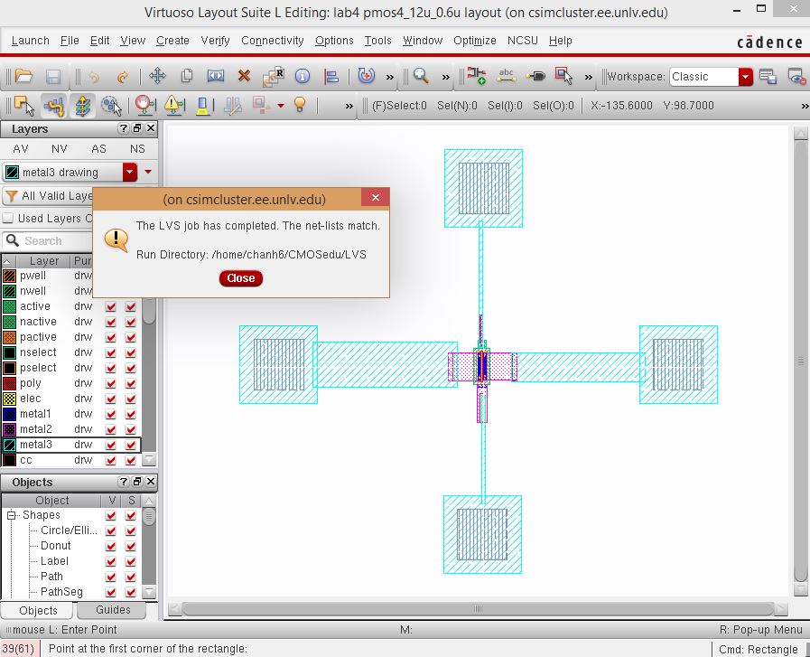
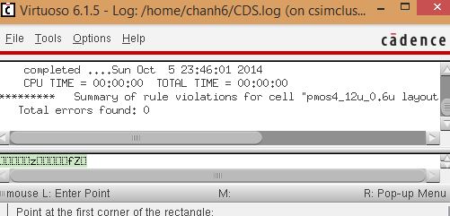
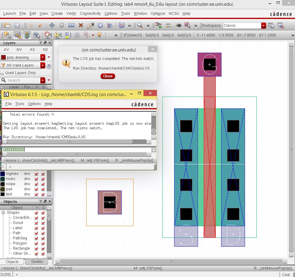
The layout DRC and LVS check out alright.
This is what the schematic looks like.