Lab 3 - EE 421L
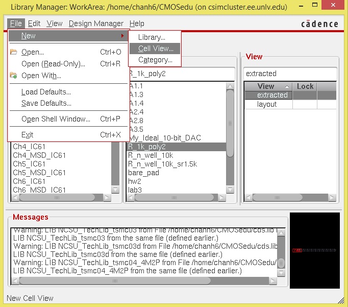
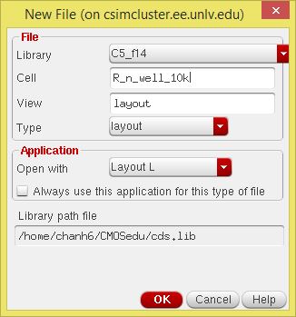
We last left off having created the symbol view of the R_div and incorporated it into the schematic for simulation. Now we are ready to create the resistor using n-well in the layout view.
Start by clicking on n-well in the layer selection window and pressing R to create a rectangle. Click and drag on the grid to create any sized rectangle, we will edit the size in a few moments.
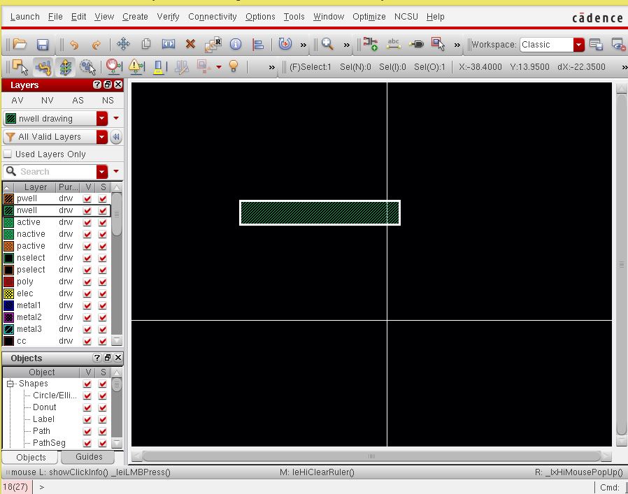
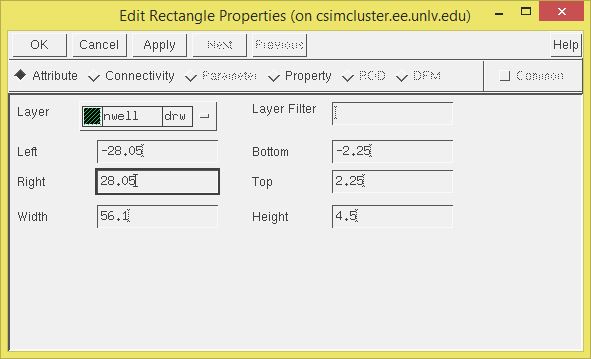
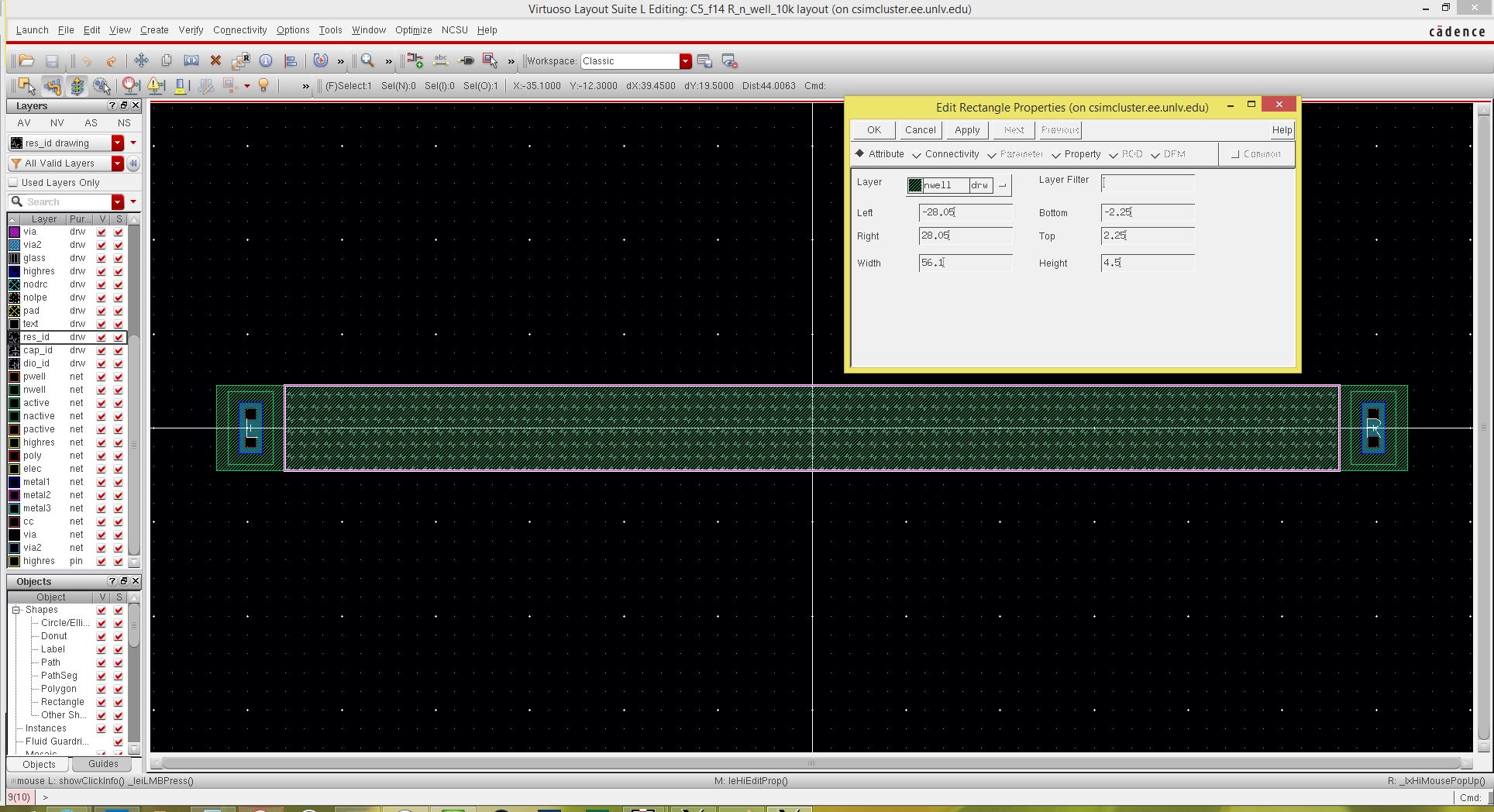
We want a resistor the be 10k specifically therefore we have to determine the appropriate dimensions of the n-well rectangle.
We can do this using this formula:
R=(R_sheet)*L/W , where R_sheet is the sheet resistance, and L and W represent length and width respectively.
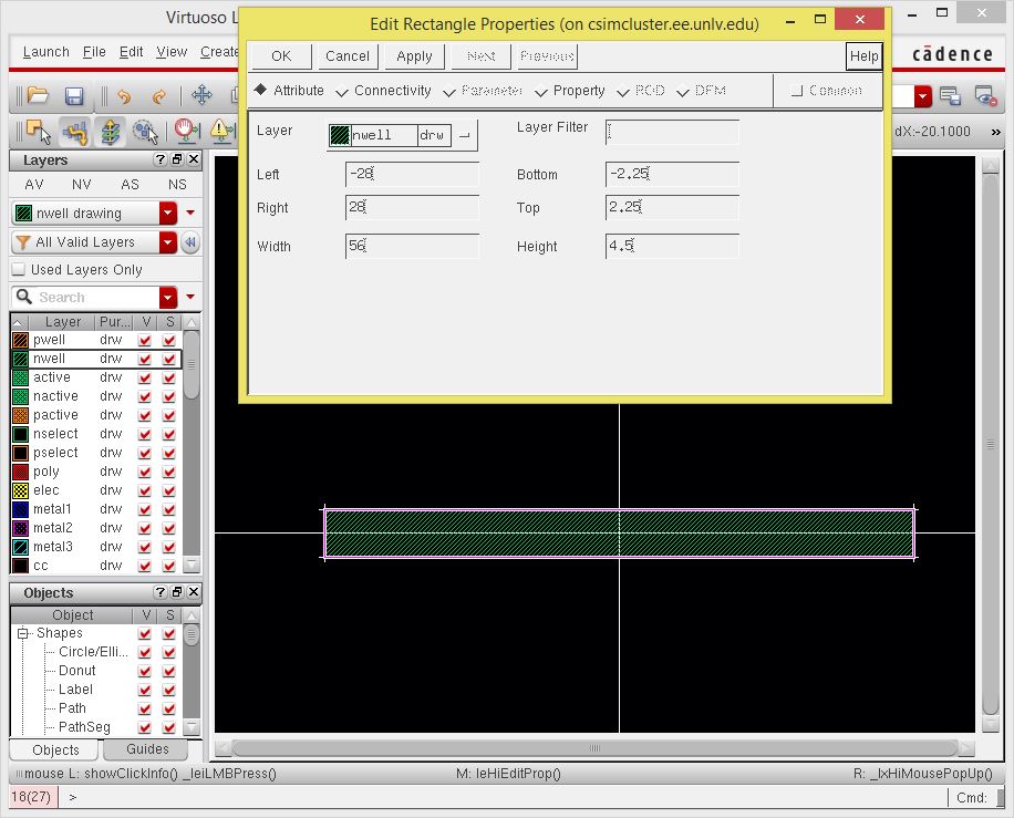
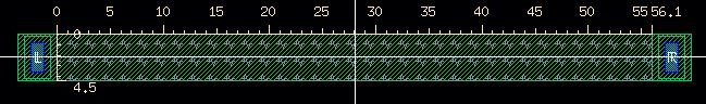
The process that we are using is ON's C5 process which says their sheet resistance for n-well is roughly 800ohms/square. Using the MOSIS submicron design rules, we know that the smallest width that we can have is 12(lambda), where lambda for MOSIS is 300nm. So we can have a minimum width of 3.6 microns. Here we will choose a width of 4.5 microns which still satisfies the rules of the process. So if we want a 10k resistor, we simply plug our values into the formula to determine our length.
10k=800*(L/4.5)=~56 microns
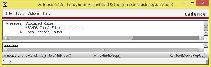
So let's see what happens when we try to Design Rule Check (DRC) it.
We receive errors!!!
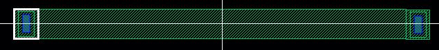
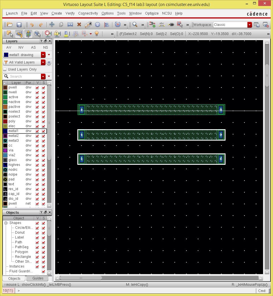
It is now time to add the ntap layers. Open the instance box by pressing I. In the NCSU_TechLib_ami06 library, select the ntap layout. This will form the connections to any metal1 layers we need, therefore it is appropriate to place it on both ends of the resistor. In the instance window, make sure to indicate two "Rows of contacts" to fit our resistor better.
You should now have something looking like this.
Now it is necessary to apply our res_id layer. Click the res_id layer in the layer selection window and press R to create a rectangle the same size as our n-well resistor without the ntaps.
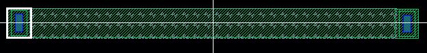
After completing the tutorial, creating the n-well rectangle, using ntap instances, and applying res_id we end up with this:
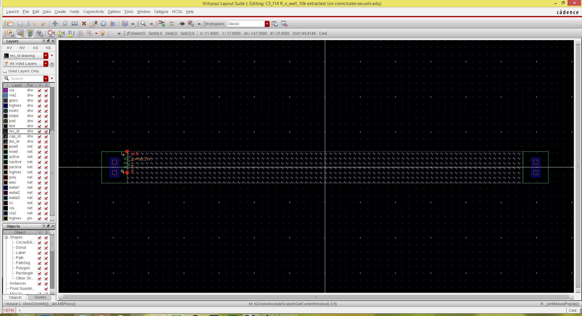
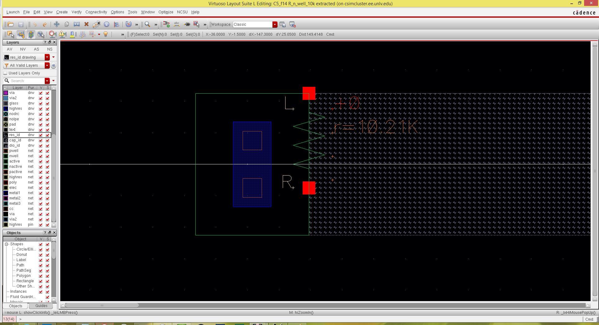
You can measure the n-well resistor's length and width by using the ruler tool (K).
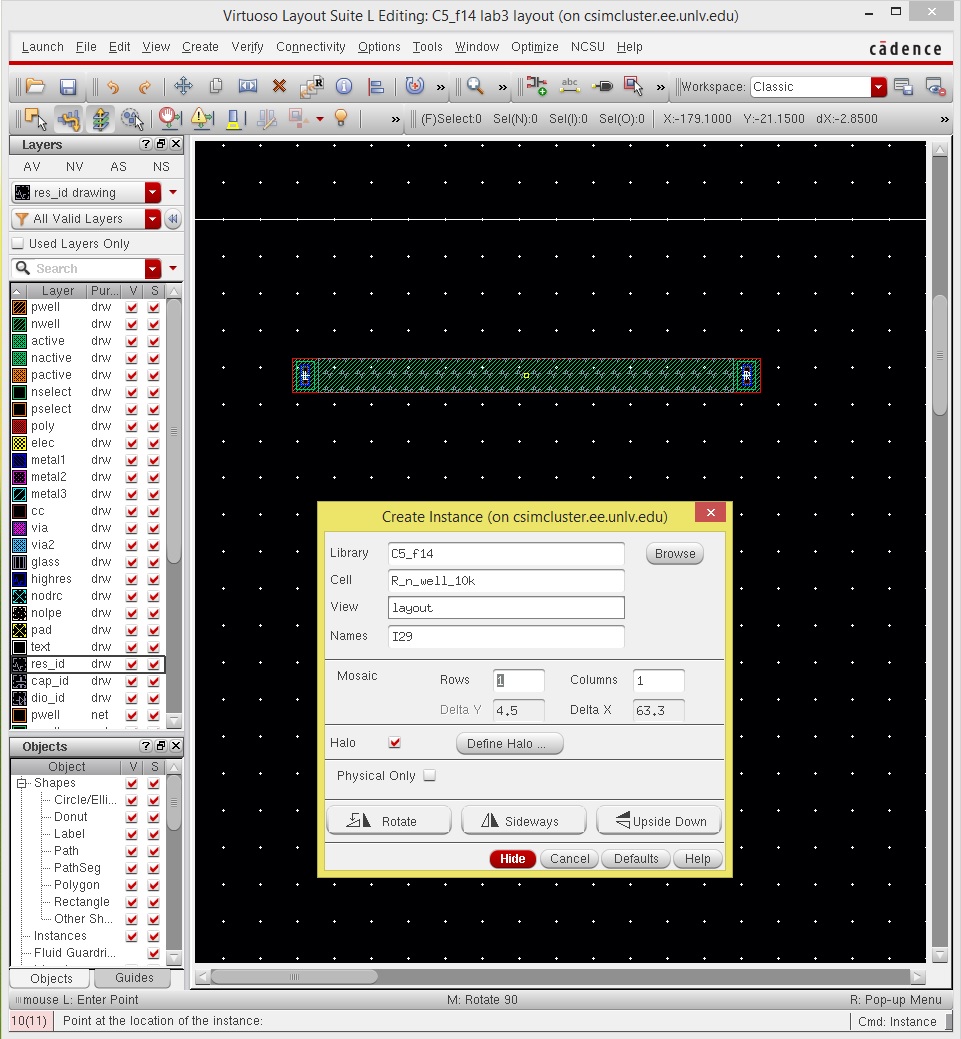
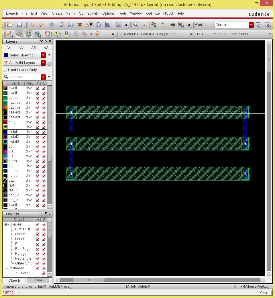
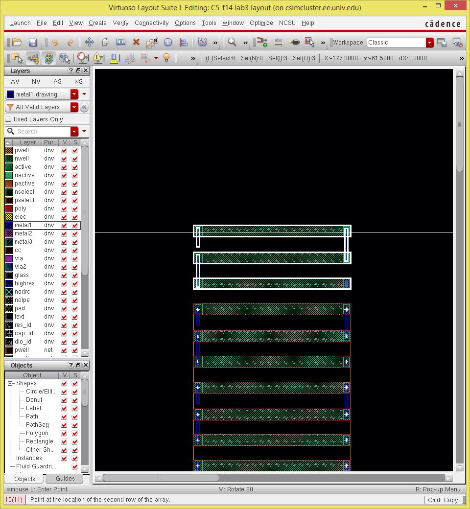
Now that the instance is created, we need more of them, so copy the current resistor layout to make a total of 3 resistors.
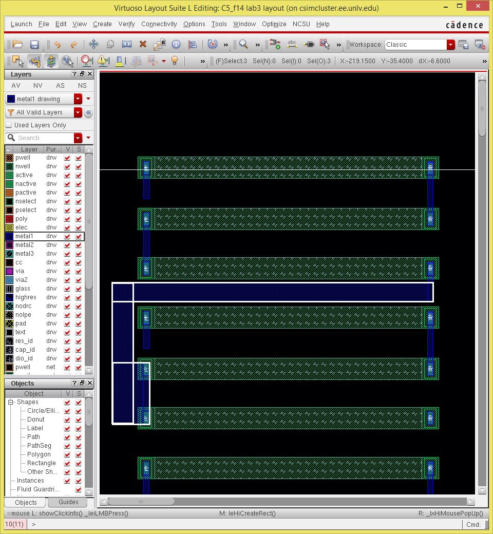
Now, we need to connect these resistors together using the metal1 layer.
This three (3) resistor configuration will form the basis or bit of our 10-bit DAC. Using this as a template, we will copy it 9 times for a total of 10 instances of a R_2R configuration as shown in the previous lab, except this time it will be in a layout view. An easy way to do this is by simply adjusting the 'Rows" parameter in the copy window.
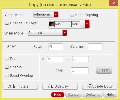
Because the lab requests the resistors be aligned along the x-axis, an orthogonal selection is perfect to maintain a stacked look of resistors.
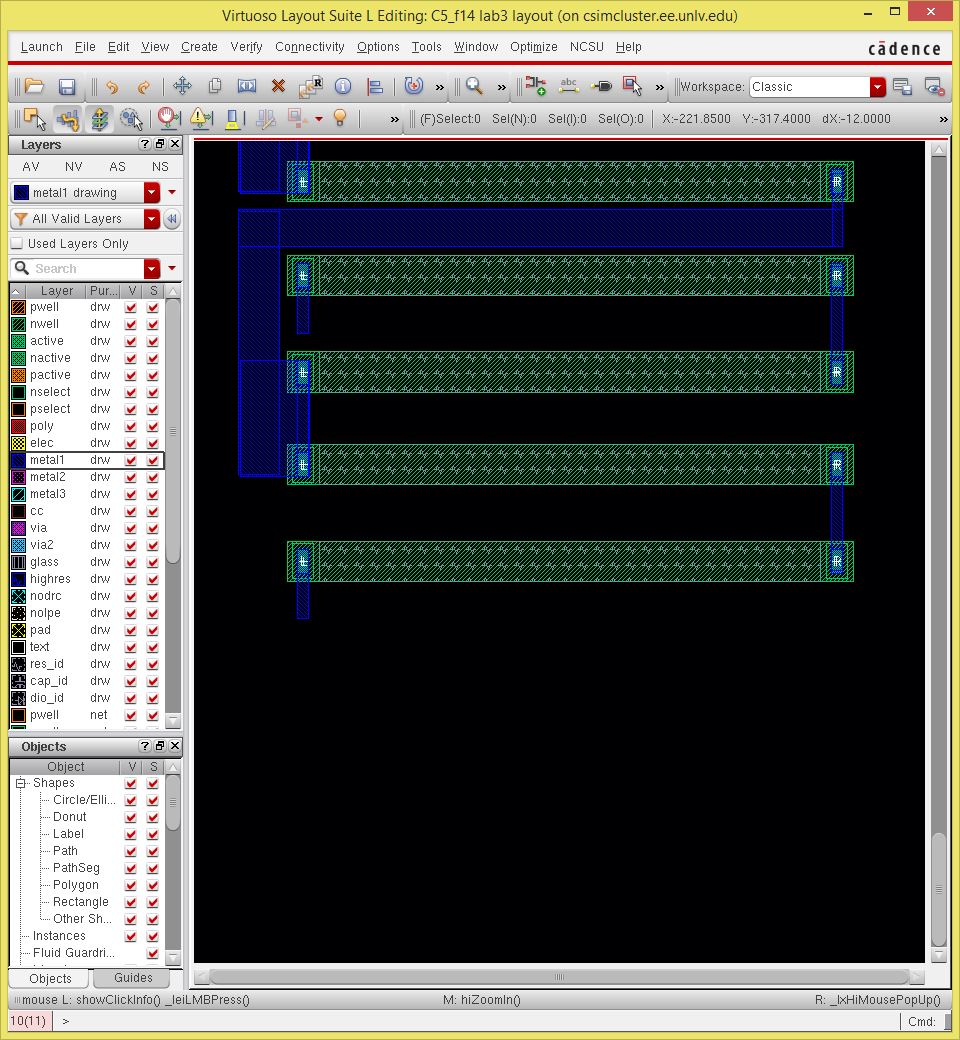
Next, we will need to connect these R_2R parts together. Do this again using metal1 using any configuration you like. An example is shown below.
Do this along the rest of the DAC.
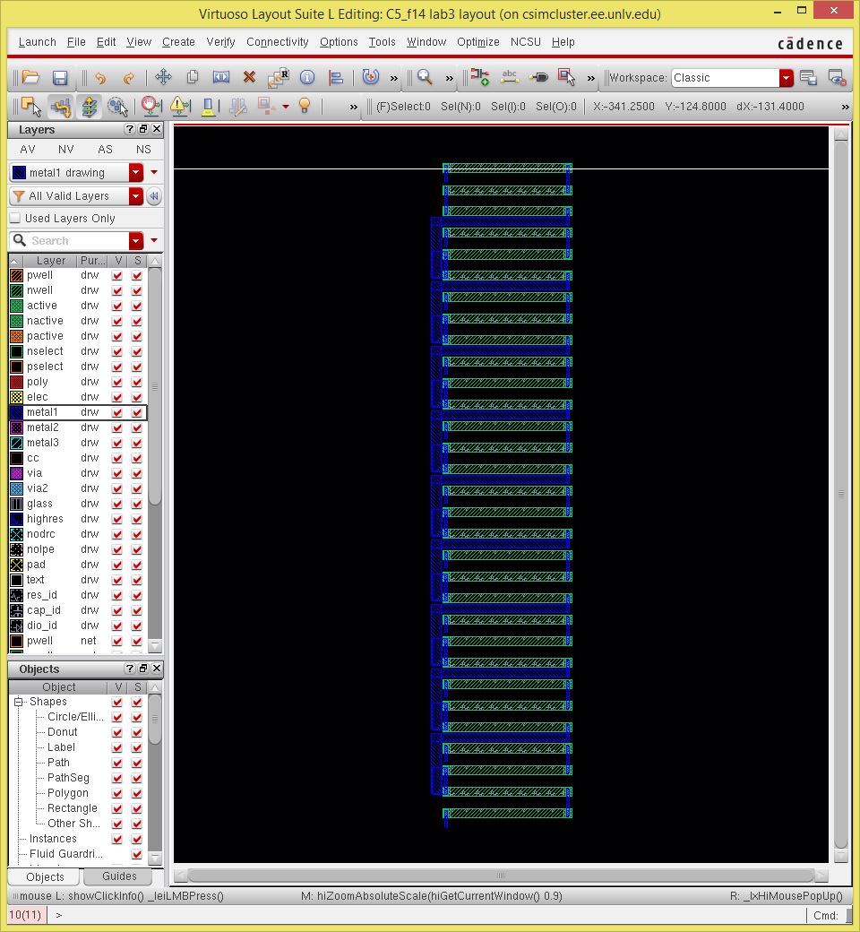
A completed version is shown above. Please note that I have added a resistor at the very end as the R_2R topology from the previous lab demands. Here is a closer look:
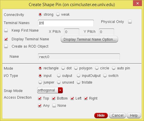
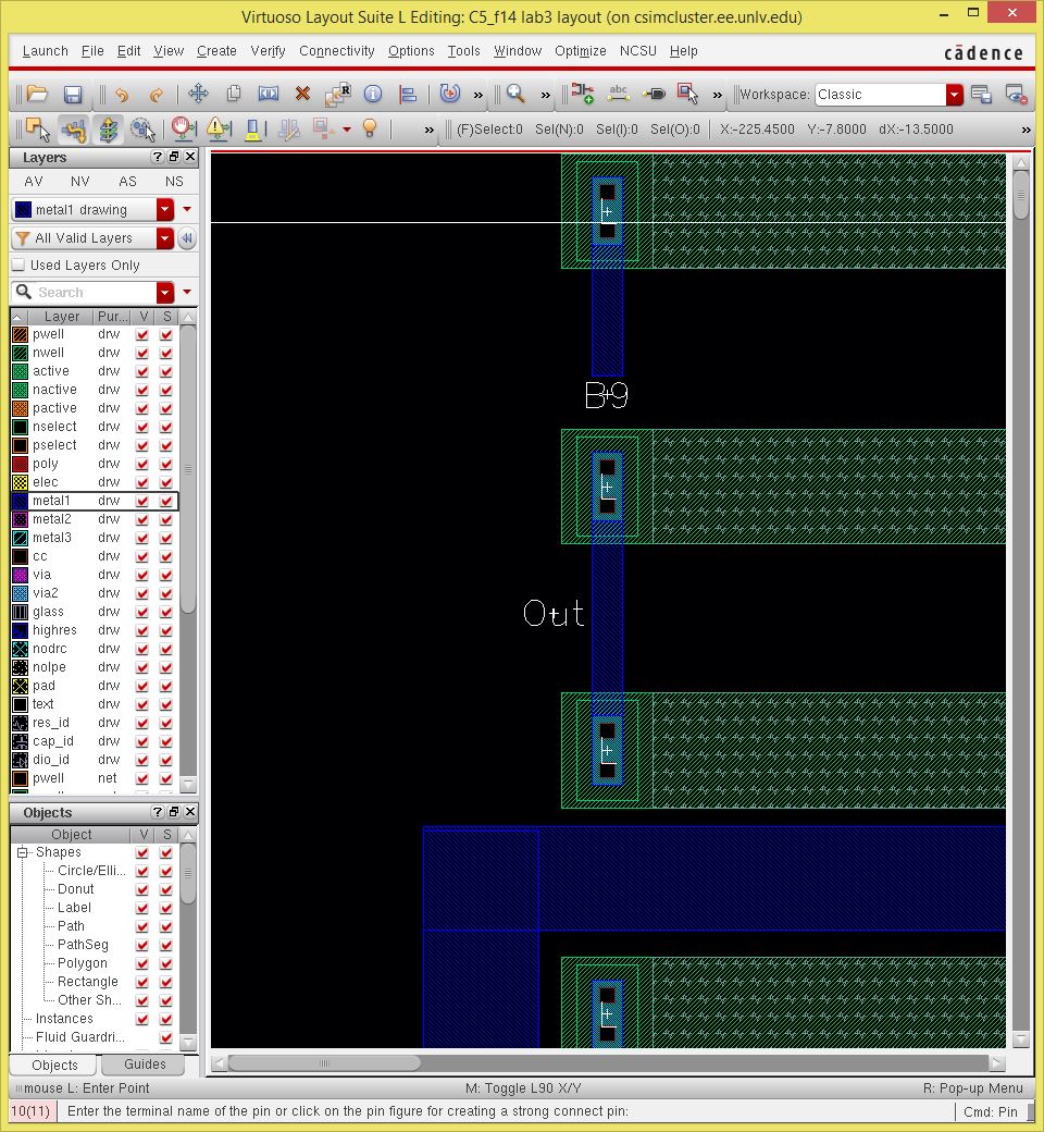
Now that we have successfully created the layout of the 10-bit DAC, we need to assign it pins! You can do this by using the Create menu and clicking on Pins (Create->Pins). Make sure the pin parameters are faithful the the schematic, or it will not LVS correctly! Also, it is useful to check "Display Terminal Name" so you can keep track of all the pins in the layout.
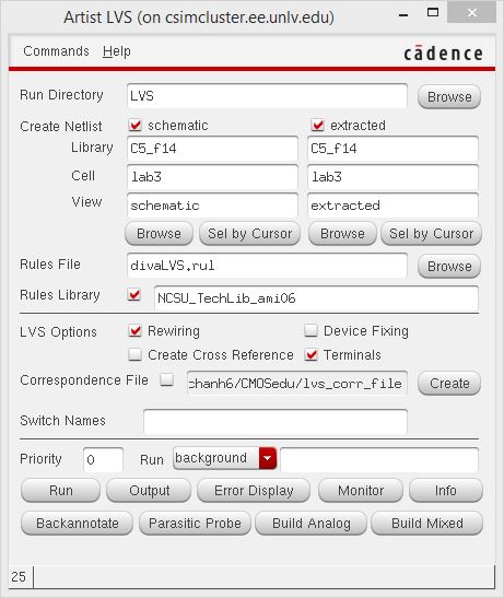
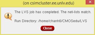
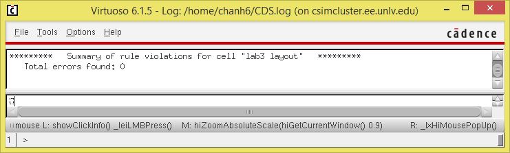
Once you've assigned all the pins, it is now time to DRC, Extract, and LVS the layout!
First DRC the layout by going to Verify->DRC. If everything goes according to play, you should have no errors!
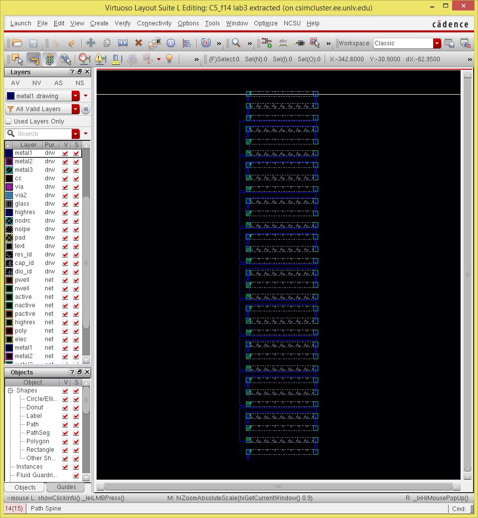
Next we need to extract the layout. Click Verify->Extract. An extracted view will now be created in your library manager. Here is what it should look like.