Lab 2 - EE 421L
Design of a 10-bit digital-to-analog converter (DAC)
Authored
by Henry Chan,
chanh6@unlv.nevada.edu
22 September 2014
The
first part of this lab aims to reproduce the steps in the prelab to
simulate a 10-bit digital-to-analog converter. The next portion
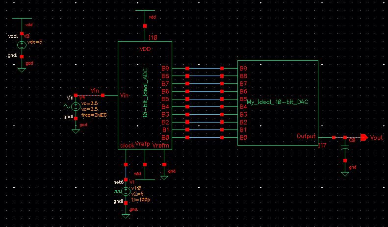
involves replacing components in the original schematic with an R,2R
resistor pattern and creating a symbol to represent the new design.
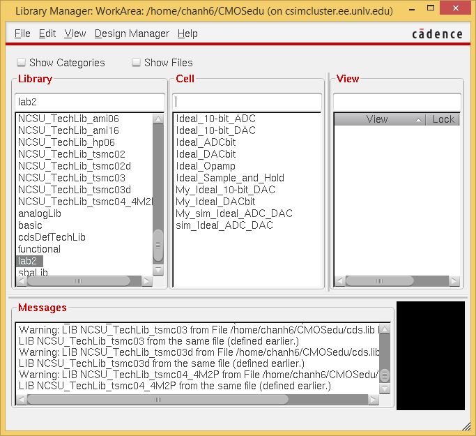
Extracting
the library into my design directory and modifying the cds.lib file to
reflect the addition allowed me to create copies of the example cells
for modification. Every cell shown with the prefix "My_" will be
altered to create a new DAC using the R,2R resistor design.
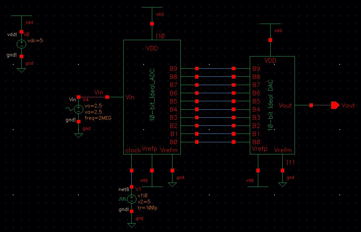
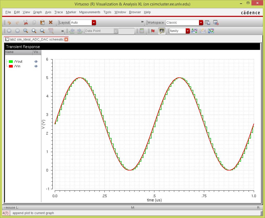
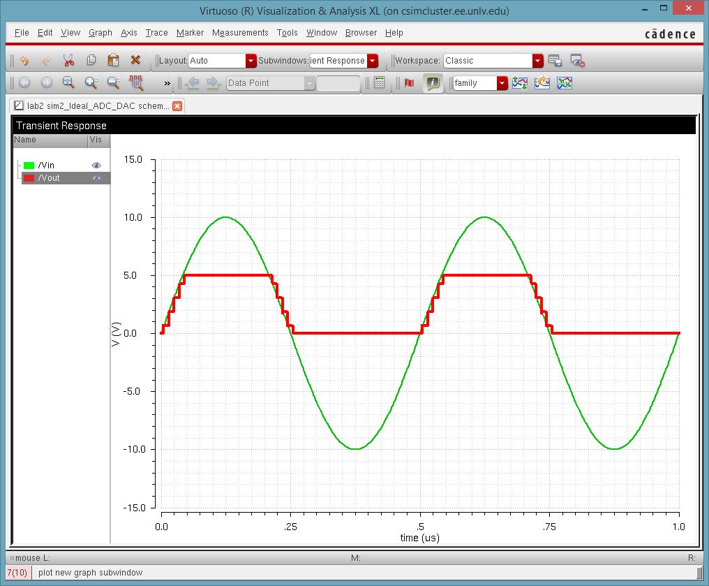
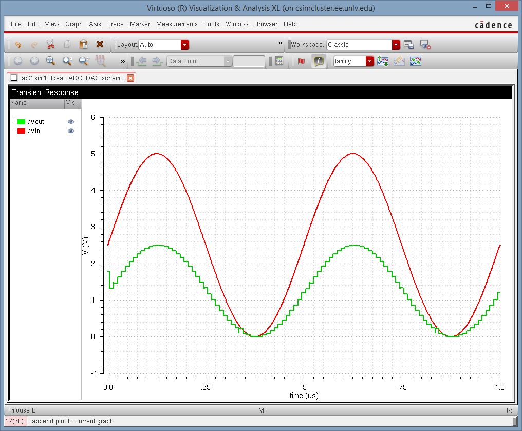
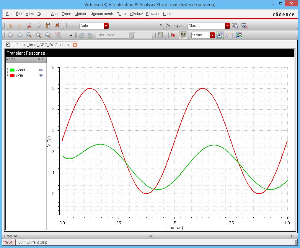
Before beginning work on my own design of the DAC, the example simulation was run to verify the function of the schematic.
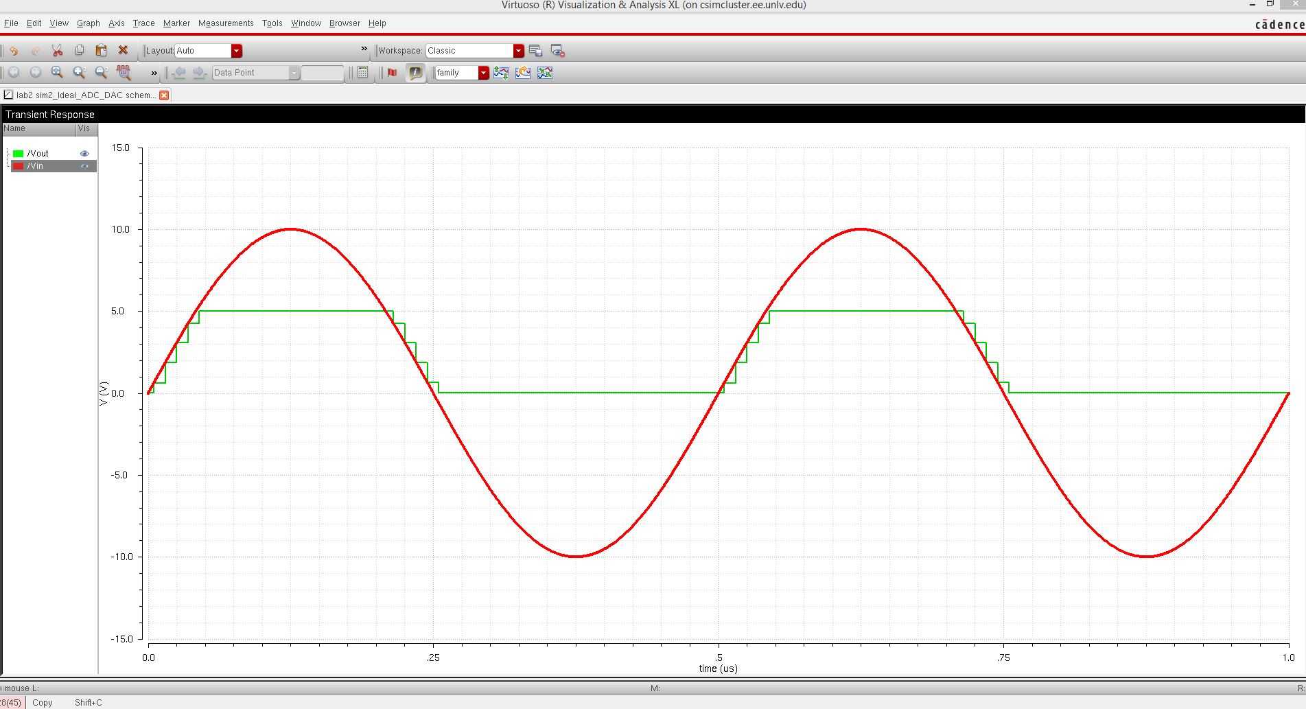
I
also modified the schematic to simulate a different output. This
different output shows the limits of the ADC and DAC; that is, it shows
that the output of the DAC is limited by the VDD given to the ADC and
DAC and can not produce a negative value.
In
order to understand the DAC more completely, I sought to know which
terminals or pins represented the most significant bit (MSB). I elected
to test B9, one of the possibilities for MSB or LSB (least significant
bit), arbitrarily. The following image shows the results of my test
simulation.
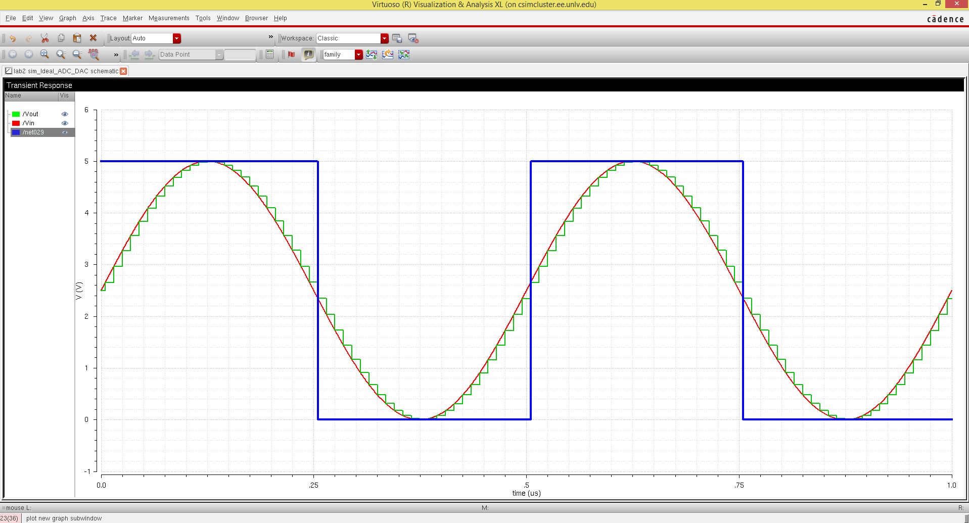
The
blue trace represents the B9 pin. It is easily determined that B9 is
the MSB because it is only high when the input and output signals are
greater than roughly half the amplitude which is how the MSB is defined
to behave. From deduction, we can also determine that B0 is the LSB if B9 is the MSB.
______________________________________________________________________________________
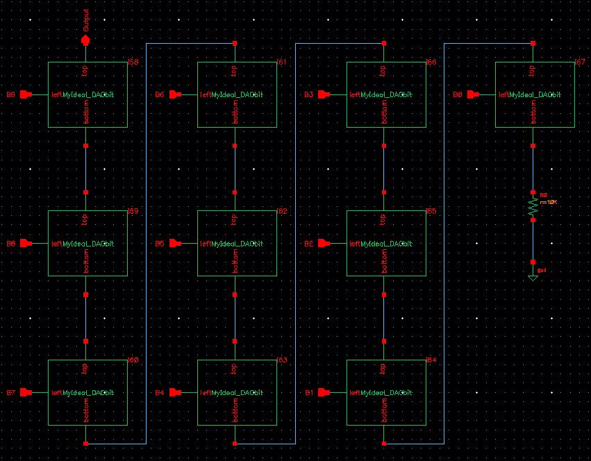
Creating a 10-bit DAC using resistors
Using the following topology as a guide, we will construct the DAC piece by piece incrementally.
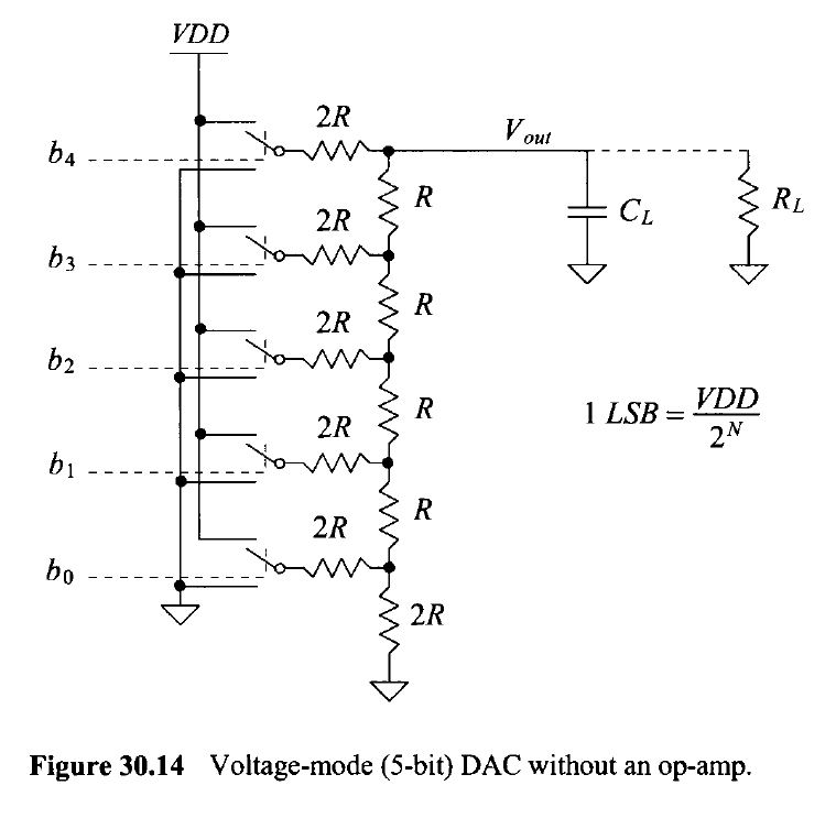
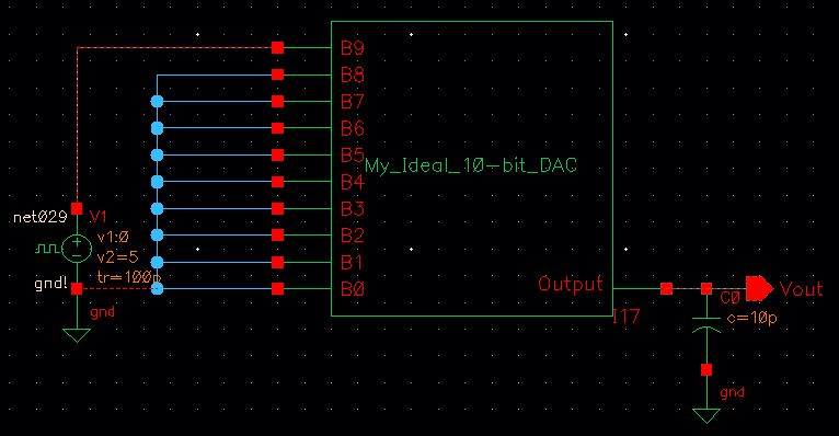
We start by creating an individual DAC bit using 10k resistors. This will provide the foundation for the further design. Notice that the ratio of resistors accurately represents the 2R and R represented above.
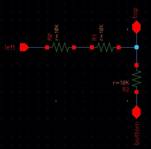
Further, we will use the symbol of this bit to represent 10 more bits.
Note the extra resistor at the very end of the chain to stay faithful to the topology.
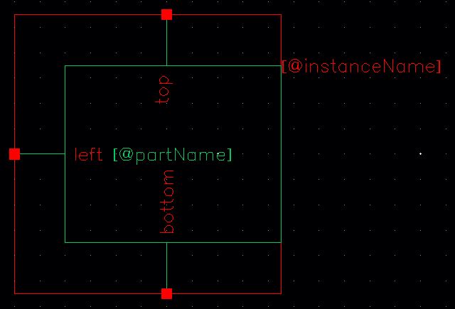
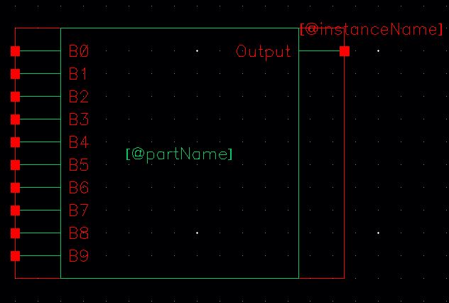
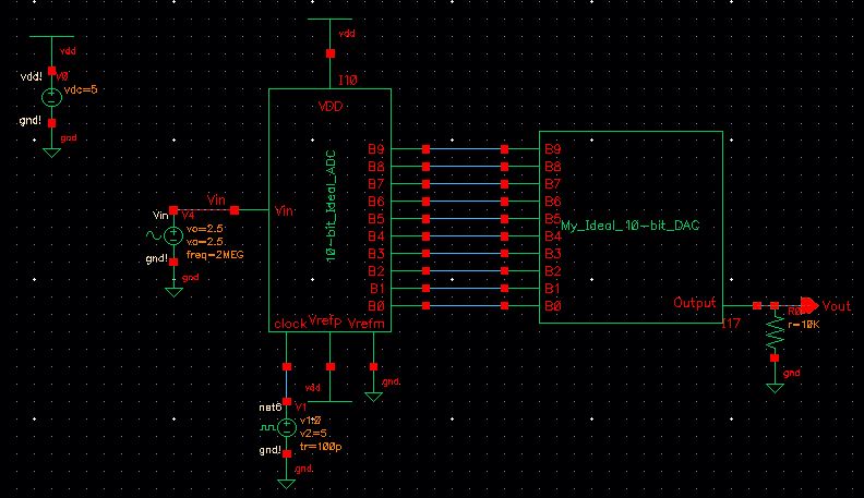
Using the above schematic, we create another symbol for easier use on a simulation schematic.
The completed DAC design in the simulation schematic.
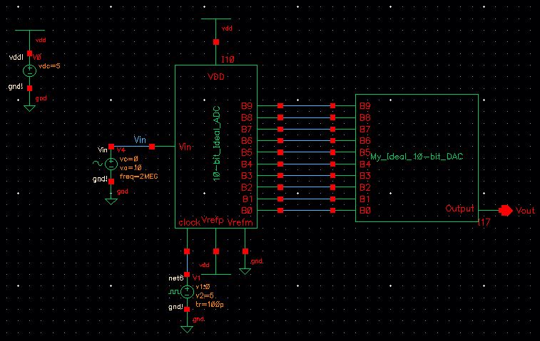
The below simulation results confirm the DAC works properly
and additionally shows the B9 bit confirming the MSB functionality.
(Modifications to the voltages to show a varied plot from the tutorial
are not shown in the schematic)
Another
test simulation verifies the limits of the DAC once again when the
input signal to the ADC is much higher than the supplied VDD..
______________________________________________________________________________________
Determining the output resistance
The
output resistance can be caluclated by shorting the floating nodes to
ground. From the bottom 2R resistors in parallel, we can see their
equivalent resistance to be R. This subsequently connects to another R
value in series. Following this pattern to the top results in a total
equivalent resistance of the topology to be R as confirmed by the lab2tutorial.
______________________________________________________________________________________
Delay, driving a load
I
proceeded to test the DAC by determining the output delay. This
involved grounding the inputs except for B9, connecting B9 to a pulse,
and attempting to drive a 10pF load. The expected output should follow
the formula for the delay of an RC circuit: 0.7RC.
0.7RC = td
0.7(10,000)(10 x 10^-12) = td
td = 70 ns
Due
to the nature of B9 being the only pin being driven, the output of the
DAC is expected to be roughly half of 5V. Furthermore, because we are
attempting to find the delay (the point at which the signal reaches 50%
of the input), we are testing for when the output voltage is 50% of the
output, in this case 1.25V.
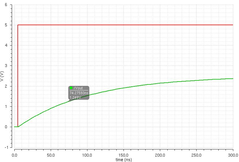
With
an initial pulse delay of 5ns, our simulated Vout is approximately on
the mark and accurate to be 1.25V around 75 ns. This is consistent with
our prediction above of a 70ns output delay.
______________________________________________________________________________________
Driving more loads!
Driving a resistor! (10k load).
This
will effectively result in the output being divided by 2 as the output
resistance of the DAC is R and the load is R as shown in the simulation
below.
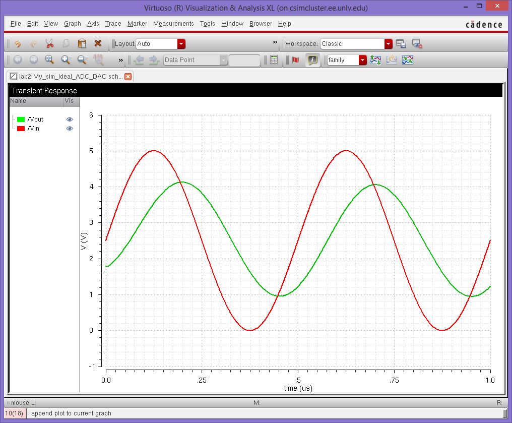
Driving a capacitor! (10pF Load)
The resulting simulation shows the output being smoothed out while also decreasing the amplitude.
Driving a capacitor and resistor! (10pF and 10k ohms)
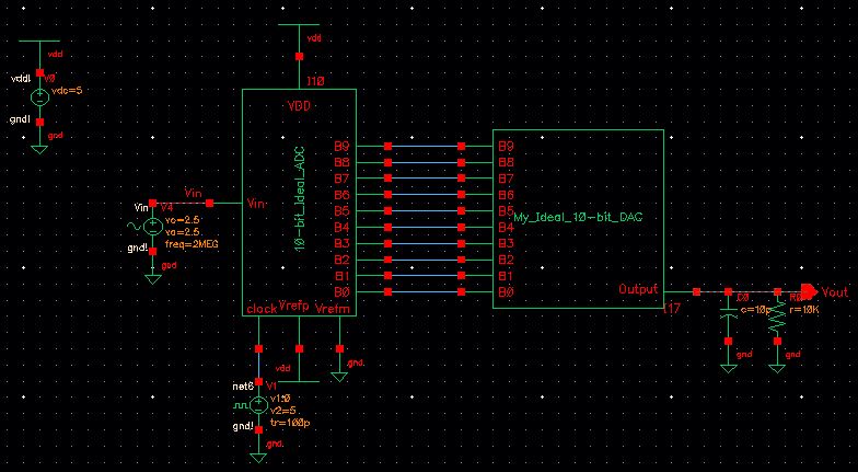
The
resulting simulation shows the smoothing out of the signal due to the
capacitor as well as the voltage division from the resistor.
In
real circuits, switches seen in the R,2R topology are implemented with
MOSFET transistors. if the resistance of the switches is not small
compared to R, the settling time increases and lowers the effective
frequency range of the circuit. The higher the resistance of the
transistors, the lower the frequencies this DAC design can handle.
______________________________________________________________
Backing up the work!
The
following image shows all the work done on this lab safely backed up
using Microsoft's OneDrive, a cloud based solution, for keeping my
files backed up.
Return to EE 421 Labs