- Go through tutorial 3.
Going through tutorial 3 will be explained below:
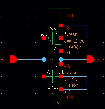
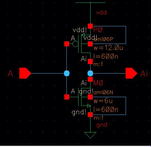
To create an inverter a PMOS4 of dimensions 12u/6u and NMOS4 of dimensions 6u/6u are used. Labels are created with input A and output Ai.
Lab 5 - ECE 421L
baldivi3@unlv.nevada.edu
Pre-Lab
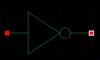
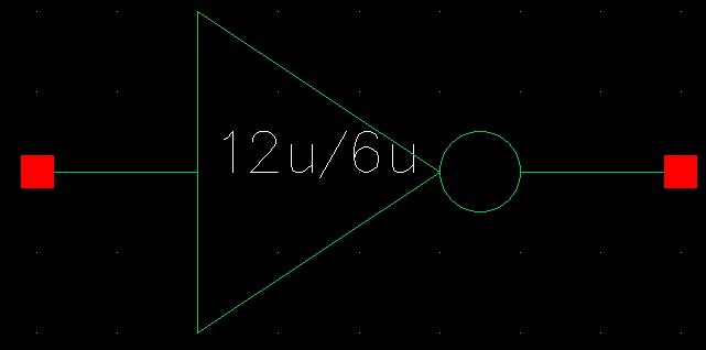
- Back up all lab work.Once the schematic is completed, going to Create->CellView->From CellView to create a symbol for the inverter. All labels are removed and the only parts left will be the pins. Drawing the inverter shape with lines and a circle will finish the symbol.
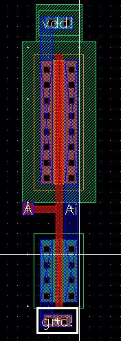
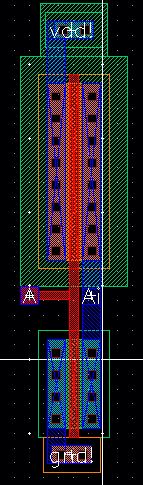
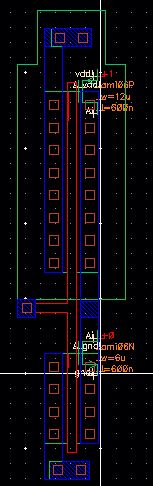
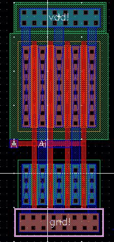
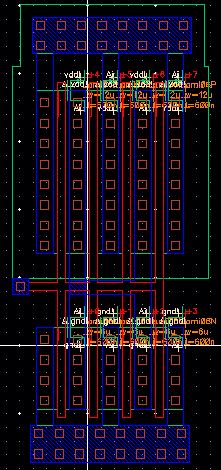
The next part of the tutorial goes through the steps of creating a layout for the inverter. Using metal1, poly, ptap, and ntap will finish the layout. Below are the images from layout and extracted.
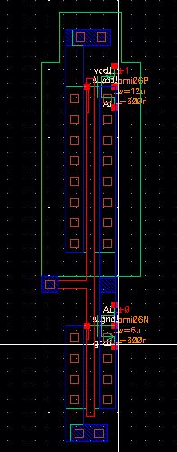
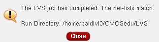
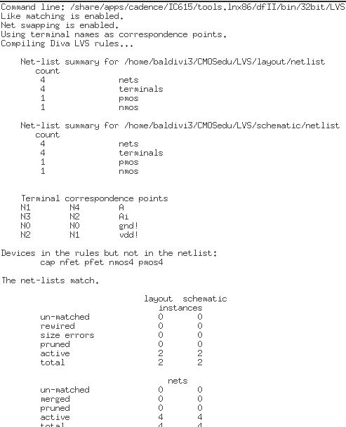
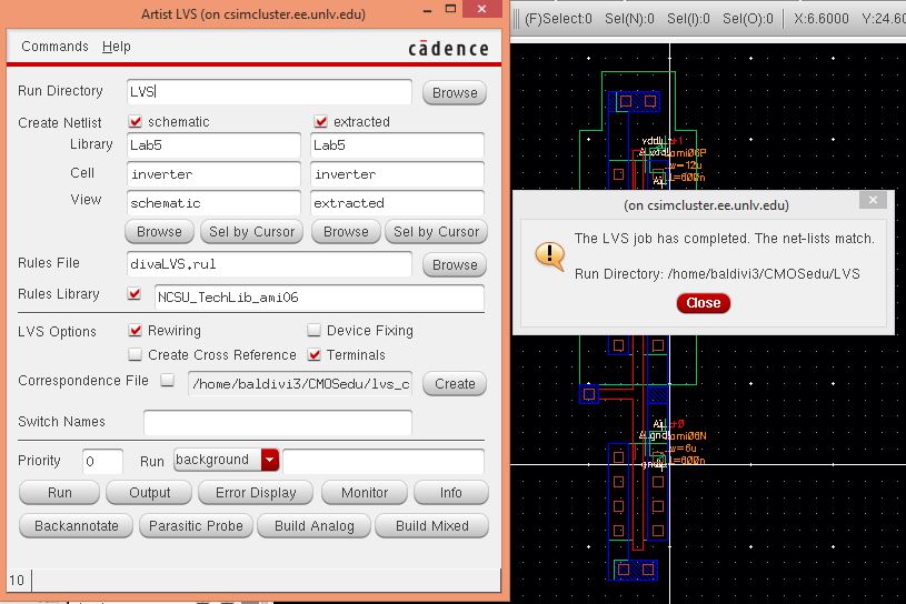
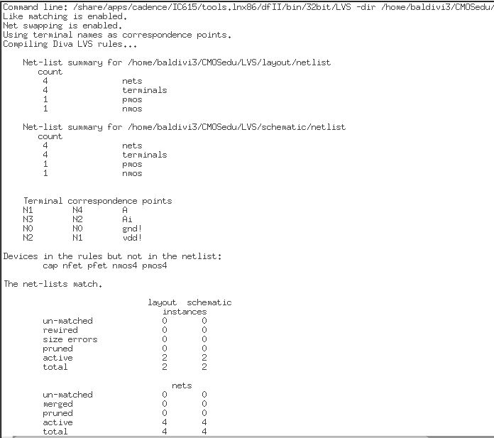
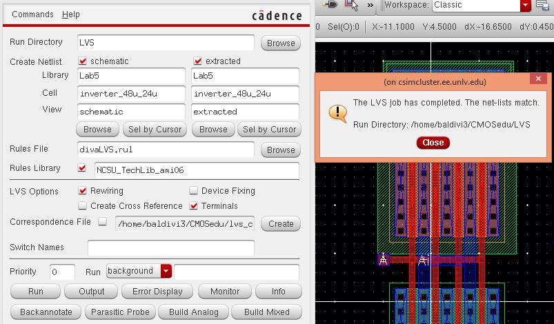
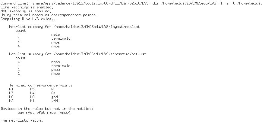
The following images prove that the LVS passed and the schematic and layout correspond.
The next step was to create a schematic using the symbol created to run a simulation.
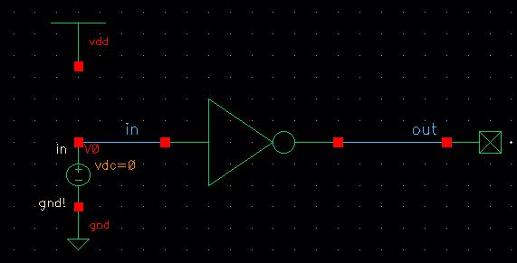
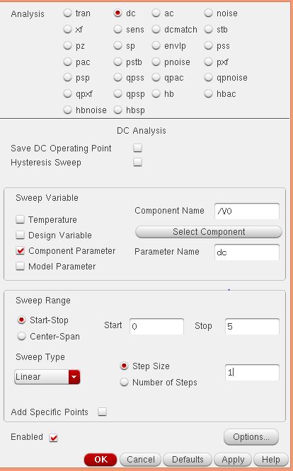
Using stimuli as directed in the tutorial, giving a dc analysis and sweeping V0 will give the following launcher.
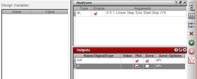
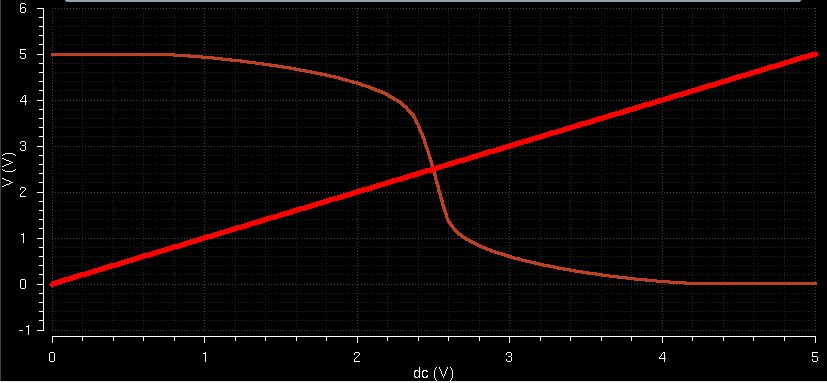
Hitting run on the simulation gives the following output.
End of Pre-Lab.
Lab
Draft schematics, layouts, and symbols for two inverters having sizes of:
- 12u/6u
- 48u/24u where the devices use a multiplier, M=4.
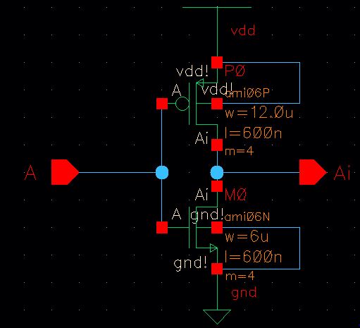
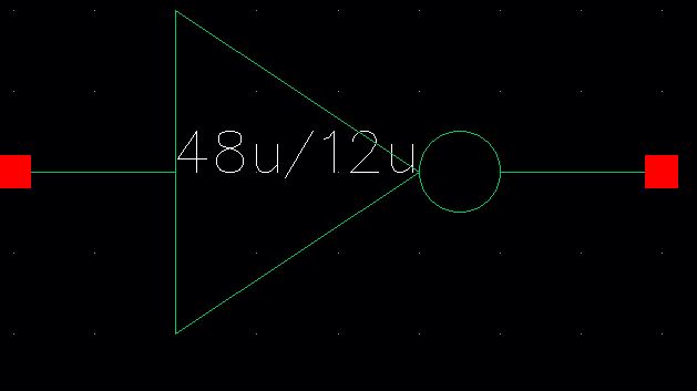
To create the 12u/6u inverter, the inverter from the Pre-Lab was used by making a copy into the Lab5 directory. A symbol was made based on the inverter schematic.
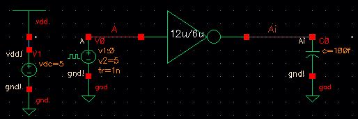
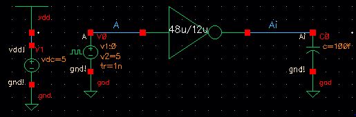
The next part of the lab requires to simulate the 48u/24u inverter. Using a vpulse with a transient analysis, the inverter symbol, and capacitors of 100fF, 1pF, 10pF, and 10pF, created the following schematic,
 (the capacitor values will change for each of the following outputs)
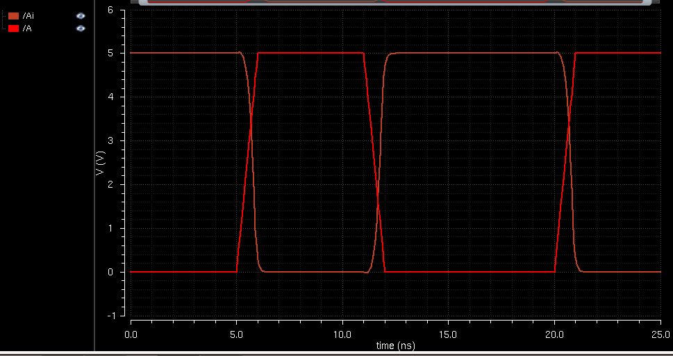
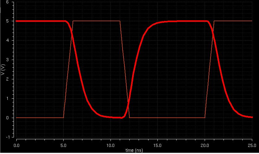
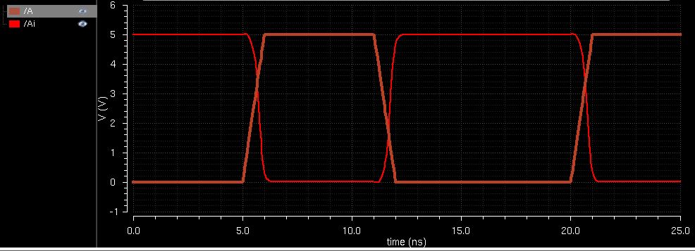
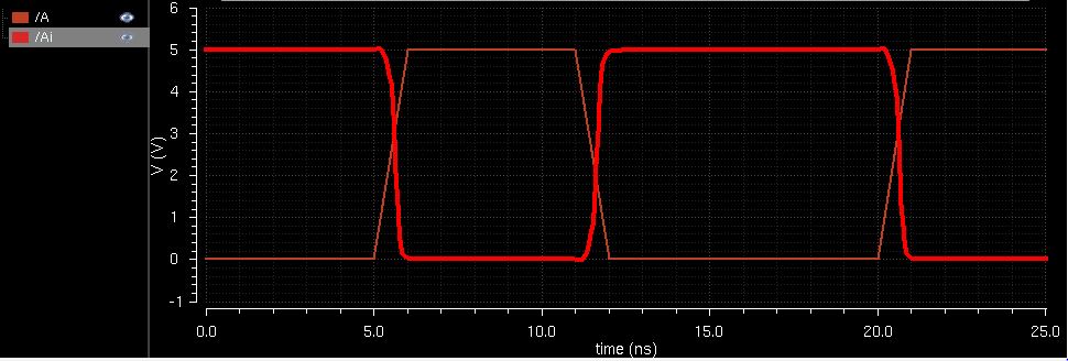
Output 100fF
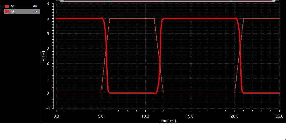
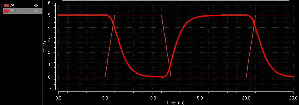
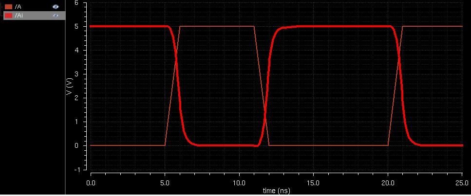
Output 1pF
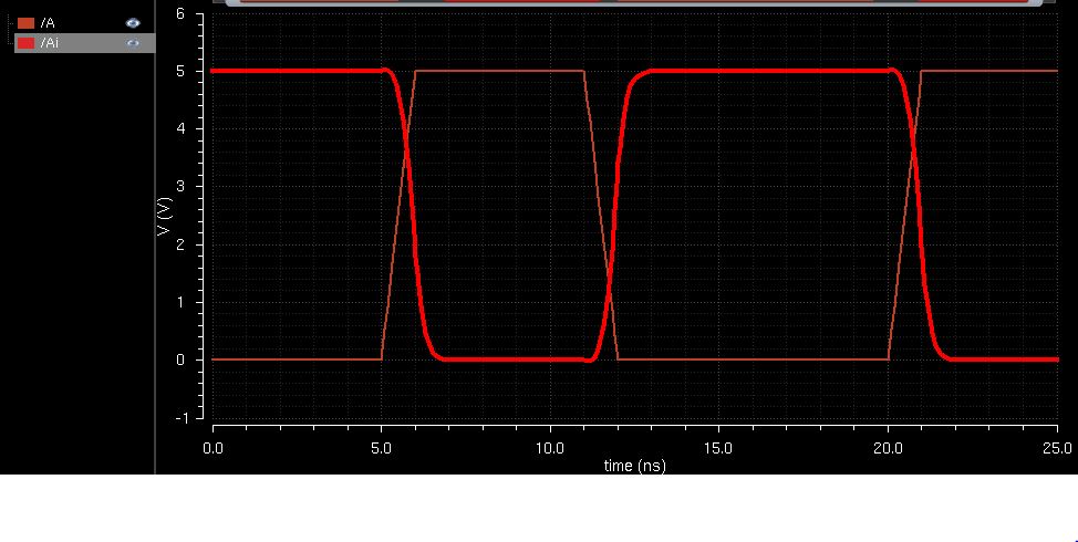
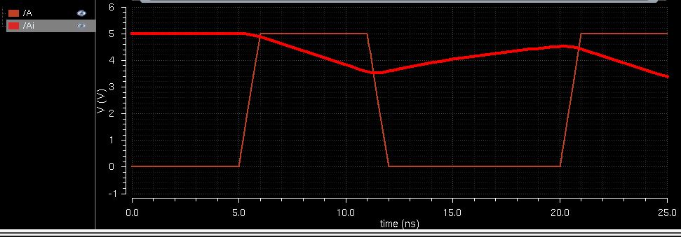
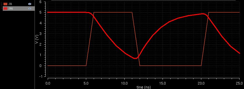
Output 10pF
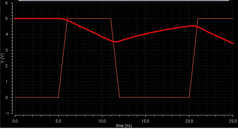
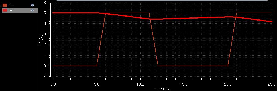
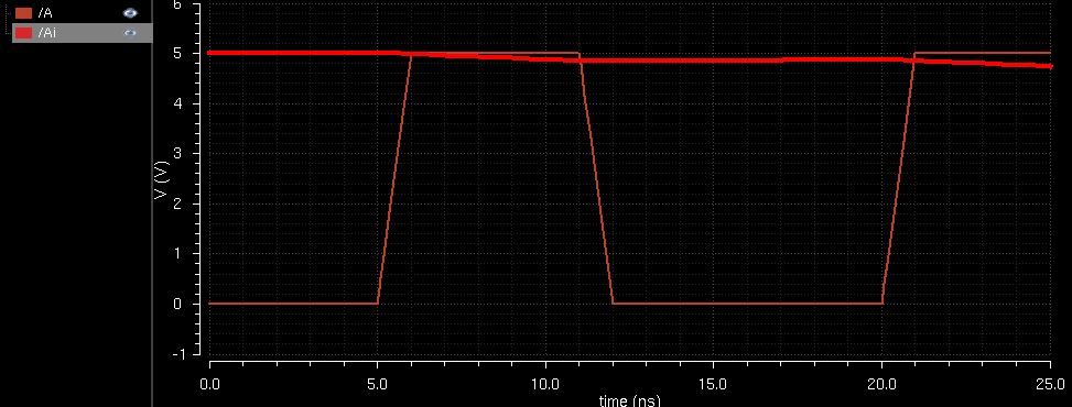
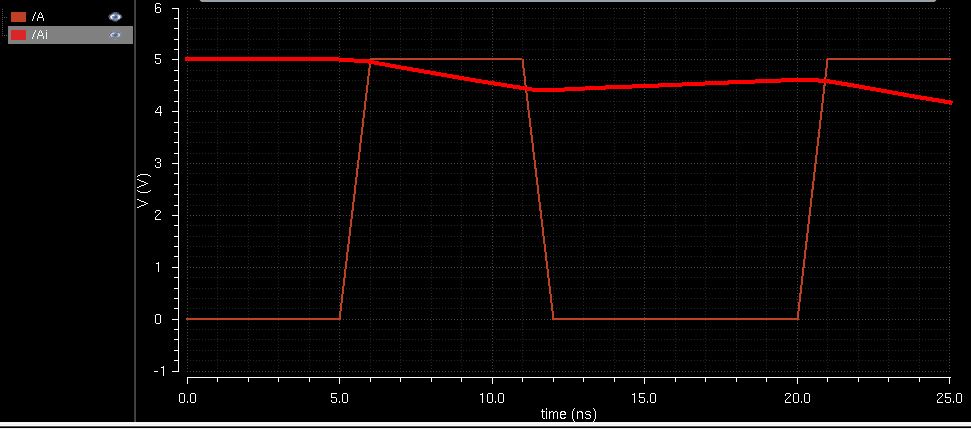
Output 100pF
Comment on the result.
The 48u/24u responds better to the higher capacitor loads than the 12u/6u inverter. In the end it is still affected by the capacitor load in that the higher the load, the less the output behaves as an inverter.
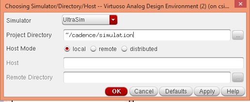
The next part of the lab was to run the simulations with UltraSim which is Cadence's fast SPICE simulator for larger circuits at the cost of accuracy.
To simulate using UltraSim go to Setup-> Simulatior/Directory/Host and select UltraSim.
Running the 12u/6u simulations using UltraSim gives the following:
Output 100fF
Output 1pF
Output 10pF
Output 100pF
UltraSim for 48u/24u inverter.
100fF
1pF
10pF
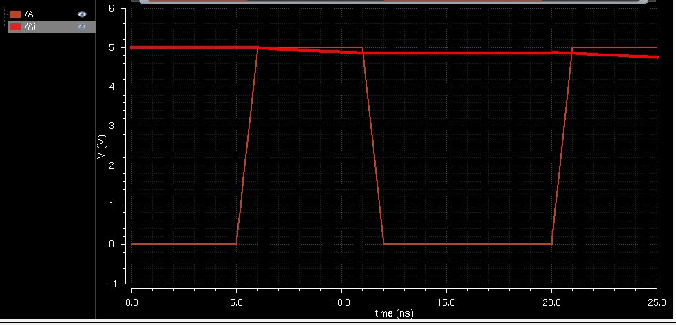
100pF
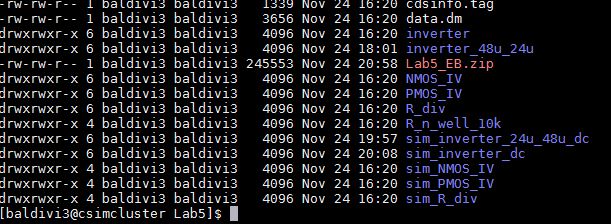
To create backups of the lab work a zip was done on the Lab5 directory in the virtaul environment. Lab5_EB.zip contains all of the cadence directories.
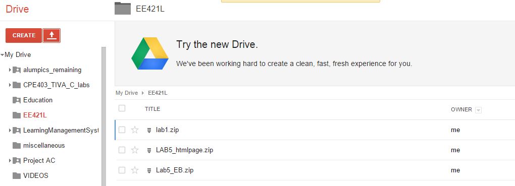
To create a backup of the webpage directory a zip was done to create LAB5_htmlpage.zip.

An upload of both directories was made to EE421L google drive directory.
Click here for Lab5_EB.zip