Lab 4 - ECE 421L
Authored
by Elizabeth Baldivias,
baldivi3@unlv.nevada.edu
IV characteristics and layout of NMOS and PMOS devices ON's C5 process
Generate 4 schematics and simulations
1.
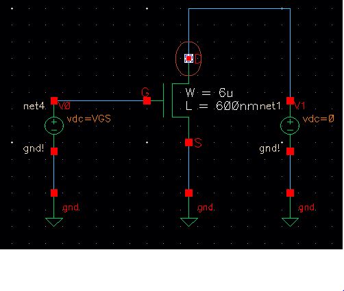
A schematic for simulating ID v. VDS of an NMOS device for VGS
varying from 0 to 5V in 1V steps while VDS varies from 0 to 5V in 1mv
steps using a 6u/600n.
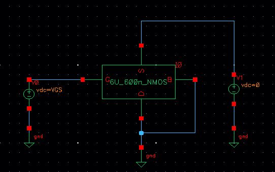
First
step was to create a schematic. I added an NMOS with 6u/600n dimensions
and added two voltage sources. One equal to VGS and the other equal to
zero.
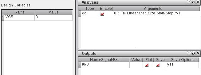
Now, I was ready to launch ADE-L. I went to Setup->Model Libraires to add ami06Nm. I added the VGS variable by going to Variables->Edit
and setting VGS to 0. I then set the analysis to dc, checked component
parameter, set the compenent name to /V1 (since that is VDS and that is
what I want to sweep). Set the sweep range to start stop from 0 to 5,
the sweep type to Linear, and the step size to 1mV. In result this is
the launch explorer.
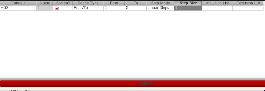
To run the simulation with varying VGS I went to Tools->Parametric Analysis and set the parameters to the ones seen below.
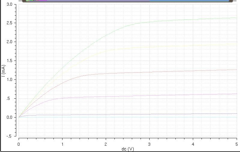
Once I hit the run button, this is the output I received.
Now, for the next task.
2.
A schematic for simulating ID v. VGS of an NMOS device for VDS=100mV
where VGS varies from 0 to 2V in 1mV steps using 6u/600n NMOS.
I
used an NMOS4 for this simulation, I set the first voltage to zero and
the second voltage to VDS. This gives the following schematic.
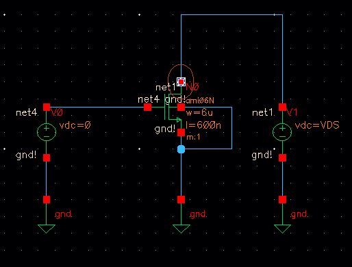
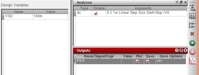
After
launching ADE-L I set the analysis to dc with component parameter. In
component name I put /V0 to linearly sweep from 0 to 2V in 1mV steps. I
added a variable VDS and set it to 100mV. This gave the following
launch.
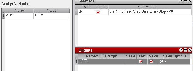
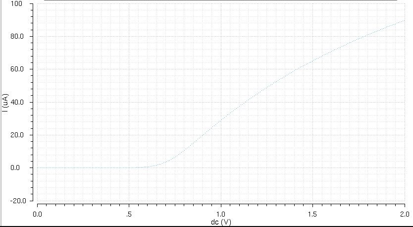
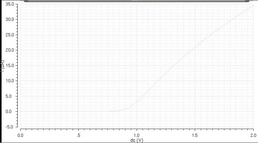
Running this analysis gave the following output.
3.
A schematic for simulating ID v. VSD (note VSD not VDS) of a PMOS
device for VSG (not VGS) varying from 0 to 5 V in 1 V steps while VSD
varies from 0 to 5 V in 1 mV steps. Use a 12u/600n width-to-length ratio.
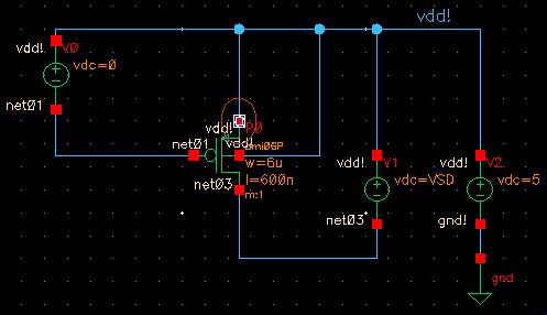
I
created the schematic for thhis simulation using a PMOS with three
voltage sources setting one of them to zero, the other equal to
5, and one equal to VSG. This created the following schematic.
This passed the check and save, now I can launch ADE-L. I made sure to go to SetUp->Model Libraries
to include ami06p. I added the VSG variable and set it to 0. I then set
the the analysis to dc, checked component parameter, set the component
parameter to /V1 since thats the voltage we want to vary, I set the
sweep to start stop from 0 to 5, the sweep type to Linear, and the step
size to 1m.
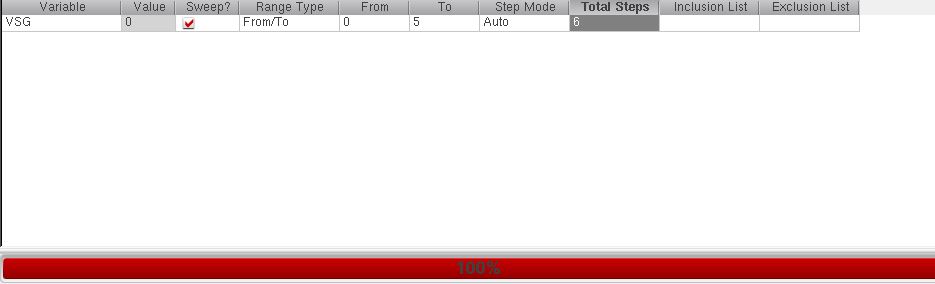
To run the simulation with varying VSG I went to Tools->Parametric Analysis and set the parameters to the ones seen below.
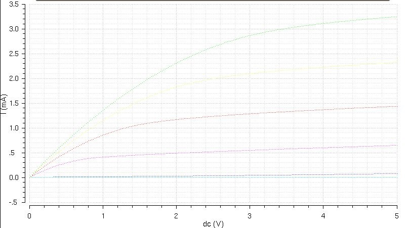
Once I hit the run button this is the output I received.
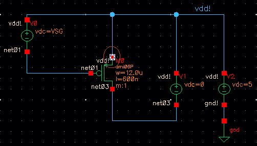
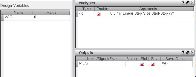
4. A
schematic for simulating ID v. VSG of a PMOS device for VSD = 100 mV
where VSG varies from 0 to 2 V in 1 mV steps. Again, use a 12u/600n
width-to-length ratio.
For
this schematic I used an NMOS4, I set the voltage that was equal to VSG
to zero. I set the middle voltage to VSD and the outside voltage to 5, giving the schematic below.
After
launching the ADE-L I set the analysis to dc with component parameter.
In component name I put /V0 since we want to be varying VSG. I set it
to sweep VSG linearly from 0 to 2 in 1 mV steps. I added the variable
VSD and set it to 100mV. This gave me the following ADE-L.
Running this analysis gave the following output.
The next part of the lab was:
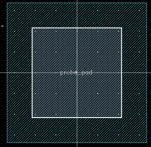
Lay out a 12u/0.6u PMOS device and connect all 4 MOSFET terminals to probe pads.
I used the examples given in the lab to do the PMOS.
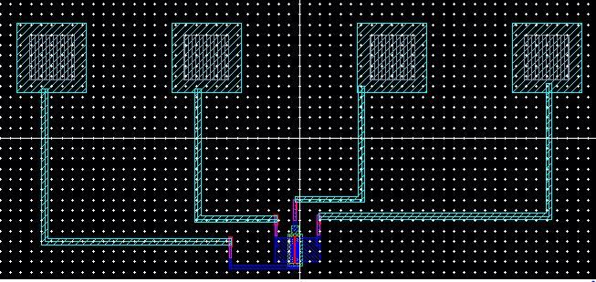
Here is the probe pad schematic and layout. The layout was made using the overglass layer and a metal 3 pin.

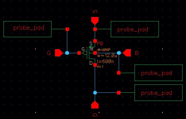
Next i needed to create a schematic for the PMOS with all 4 terminals connected to probe pads.
Now
the layout was needed. I created the layout using metal 1 to connect to
the PMOS gates. The metal 1 connected to metal 1 that went to the probe
pads, using m2_m1 to connect m1 to m2 and then using m2 to connect to
the metal 3 on the probe pads. Here is the result with verification of
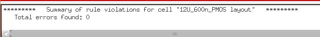
passing DRC.
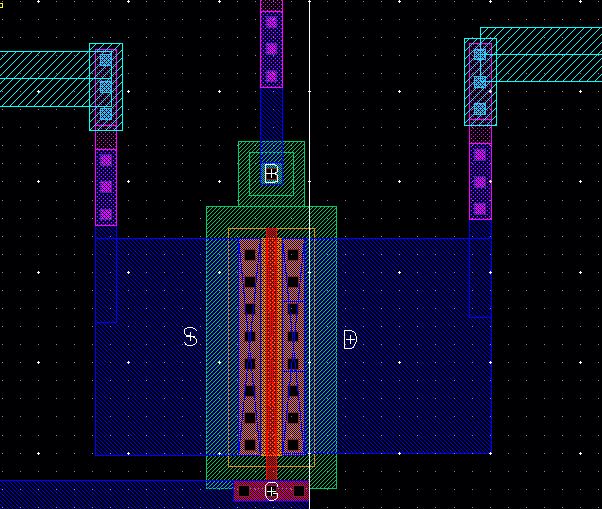
Here is a close up of the PMOS connections.
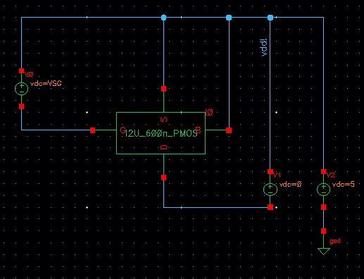
Next I used the symbol that includes the probe pads and PMOS to create a schematic for getting the I-V curves.
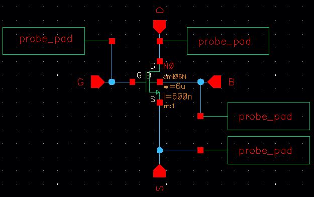
Lay out a 6u/0.6u NMOS device and connect all 4 MOSFET terminals to probe pads .
For
this I used the same probe pad schematic and layout. I used the PMOS
schematics I had already created and just replaced the PMOS with NMOS
and renamed the pins to get the following.
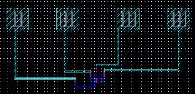
To
create the corresponding layout I used the previous layout I created
for PMOS and removed the PMOS and put an NMOS. I added an ntap and also
added metal 1 connections to connect to the metal 1s that take you to
the probe pads. I created pins for the metal 1 connections i created. I
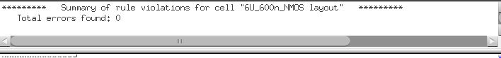
also verified that it passed DRC.
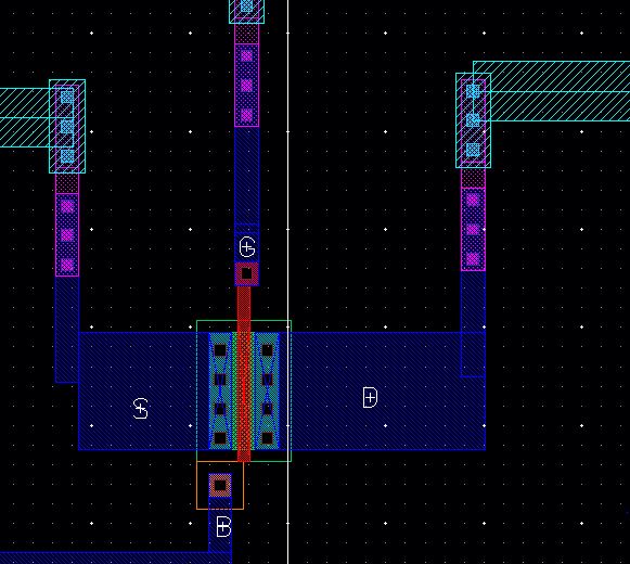
Here is a close up of the connections to NMOS.
Next I used the symbol that includes the probe pads and NMOS to create a schematic for getting the I-V curves.
I created a back up of my work and zipped it up into lab4.zip. I then emailed a copy to myself.
Return to EE421L Labs