Project - ECE 421L
Elizabeth Baldivias
baldivi3@unlv.nevada.edu
The purpose of this project was to design, layout, and simulate an 8-bit ALU that can perform:
A AND B
A OR B
A+B
A-B
Project Part 1
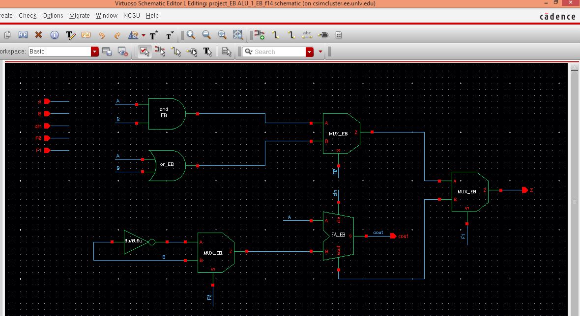
The
first part that I created was a 1 bit ALU. It consisted of the
components shown in the schematic. The control signals are F0 and F1.
To set the ALU to perform A "AND" B I set F0 and F1 both equal to 1,
therefore 11. To set the ALU to perform A "OR" B I set F0 and F1 to
01. To set the ALU to perform A+B, I set FO and F1 equal to 00. To set
the ALU to perform A-B I set F0 and F1 to 01.
To
enable the ALU to perform subtraction I had to connect an inverter to a
MUX that will go into the full adder B input. This is done because in
binary subtration is not done, therefore the 2's compliment has to be
taken.
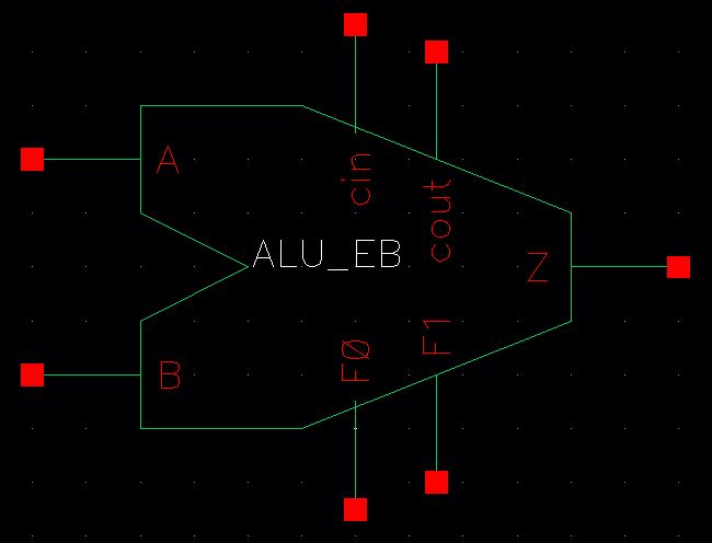
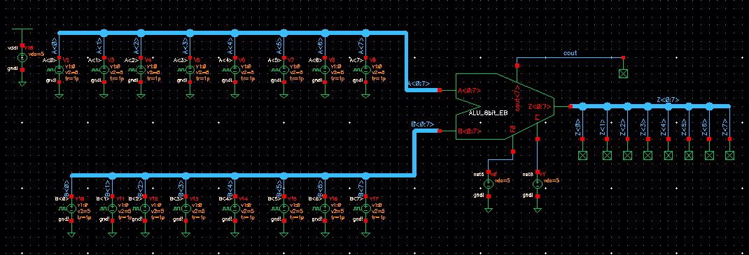
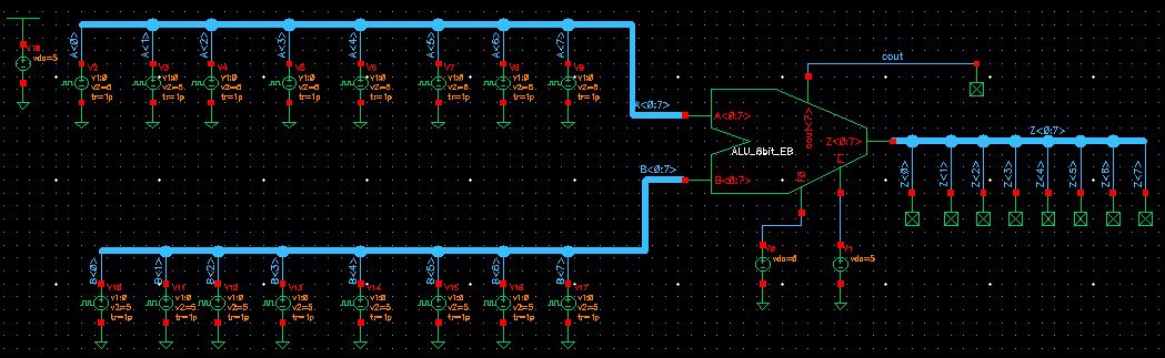
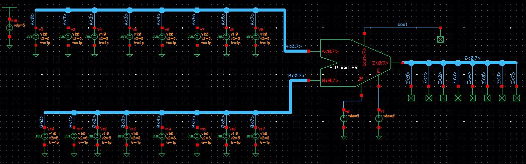
Once the schematic was created, a symbol was made in order to be able to use that symbol to create the 8 bit ALU.
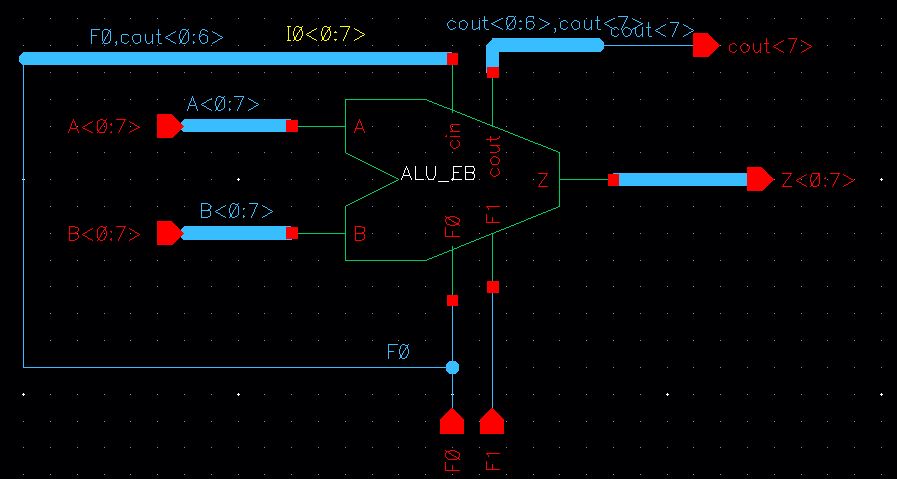
Once
the symbol was created a schematic was made for the 8 bit ALU. It was
done by adding wide wires and naming them with the array naming
convention. In order to only have one full adder in the schematic we
connected F0 to cin. By doing this when you a put 1 or 0 in the F0 pin
it will determine if the full adder will perform subtraction or
addition.
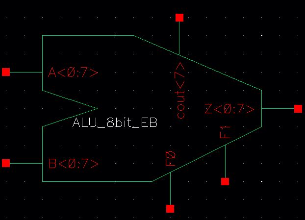
In order to perform the the ALU operations, a symbol of the 8 bit ALU was made to be able to instantiate the 8 bit ALU.
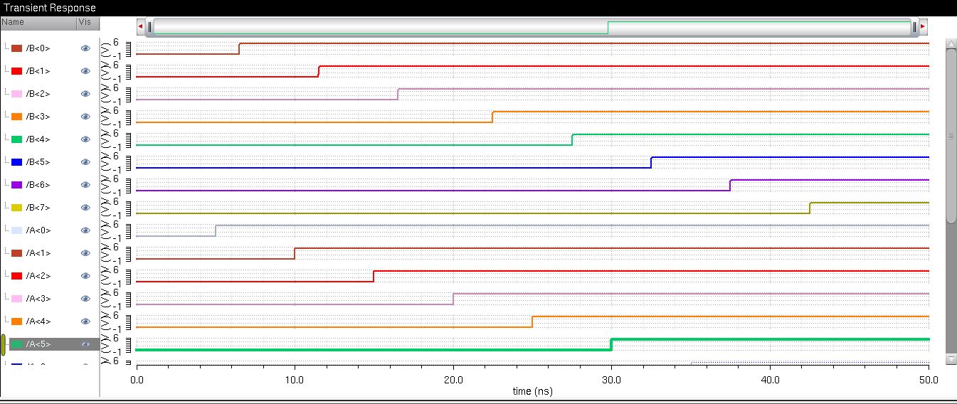
To
create a simulation of the AND operation I set F0 = 1 and F1 = 1 which
meant to set both the vdc's connected to F0 and F1 to 5. I created an
array of 8 inputs for B and an array of 8 inputs for A. To have
different combinations I added vpulse and set different time delays to
each one. The 8 bit output was connected to no connects to create the
following simulation.
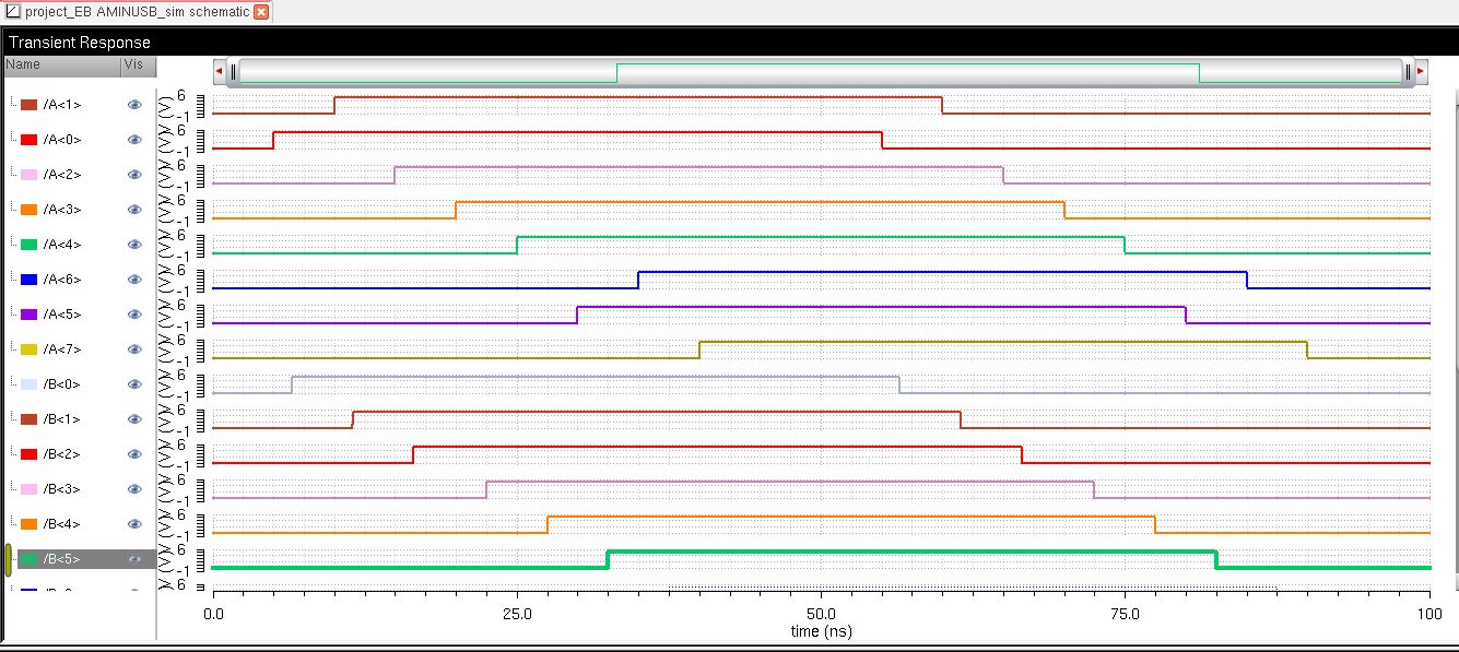
The following two images show the inputs and outputs of the simulation.
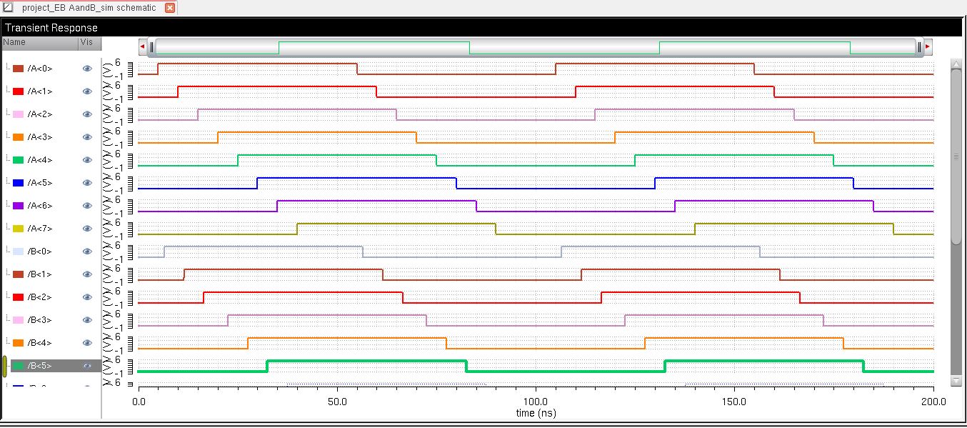
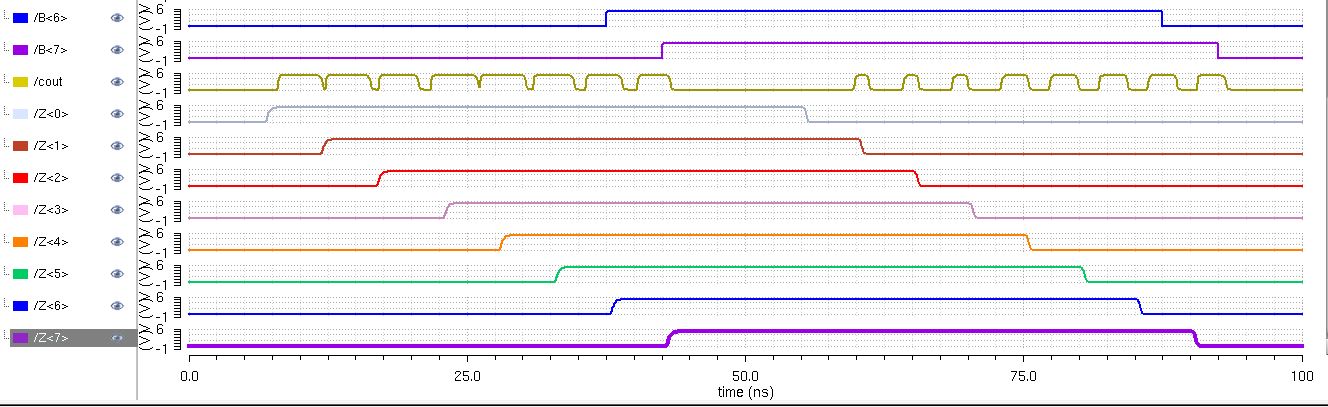
At
70 ns (about 3 ticks to the right of 50 ns ) A= 11111000 and B =
1111000. Looking at the output Z it was equal to 11111000. Therefore
the ALU is performing correctly.
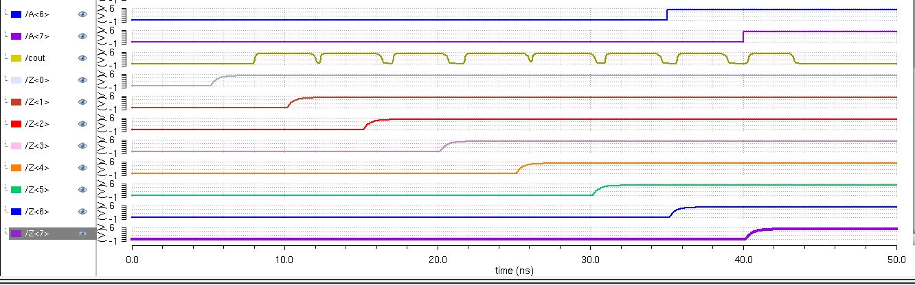
The next operation I tested was
A plus B. I used the same schematic, but changed F0 and F5 equal to
zero to perform the addition. The following two images are the inputs
and outputs.
At
40 ns A = 11111111 and B = 11111111. Adding up A plus B will give you a
totoal of 510, even though the output z = 11111110. The circuit is
still working correctly because cout is equal to 0 and taking into
account that 0 will end up giving the correct output which is 11111110.
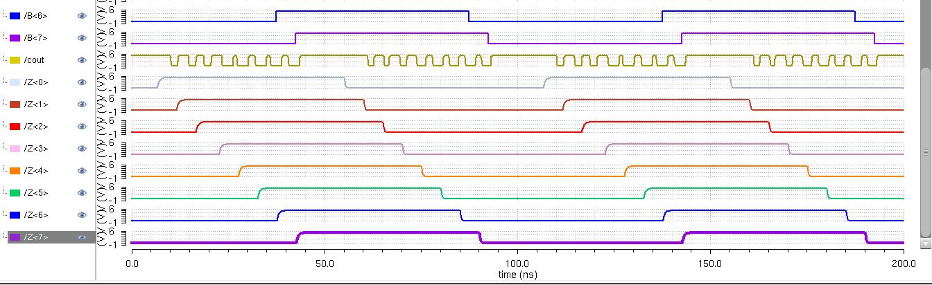
The next operation to simulate is A or B. To get the AorB output I set F0 and F1 = 5V.
The following 2 images are the outputs.
At
10 ns A = 00000011 and B = 00000001. A or B = 00000011 which is what
the z outputs turn out to be therefore the ALU or operation works.
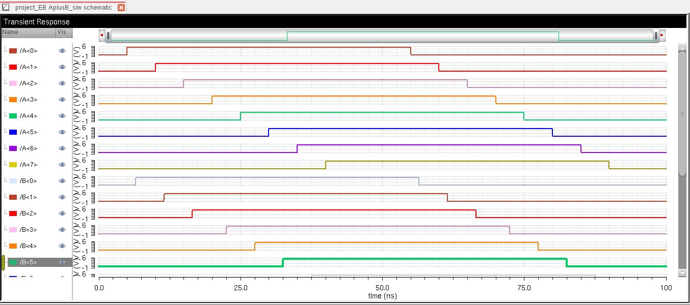
The last simulation to do is A minus B. To perform this operation I set F0 = 5v and F1 = 0v.
The following two images are the given outputs.
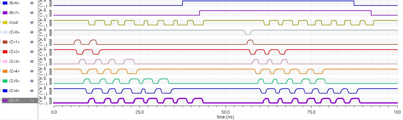
In
this simulation at 50 ns, A = 11111111, B = 1111111 with cout = 1 that
means the 2's compliment of the output has to be done to z. z is given
as the correct output.
Project Part 2
In this part of the lab the goal was to create a layout of the 8 bit ALU.
I started by creating the 1 bit ALU layout.
Before I did the 1 bit ALU layout, I created the layouts for each 1 bit component of the ALU.
AND Layout
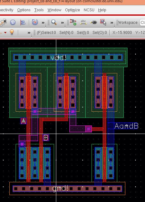
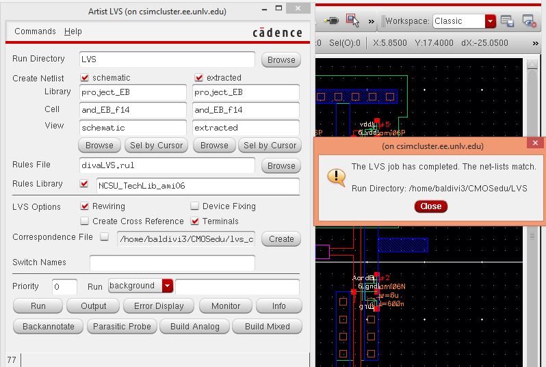
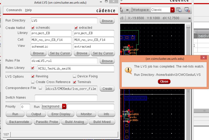
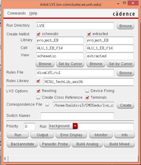
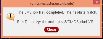
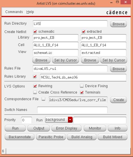
I verified that it passed LVS.
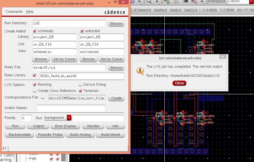
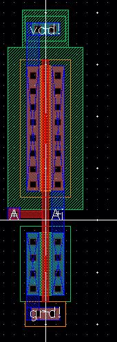
OR
Again, making sure that LVS matches.
Inverter
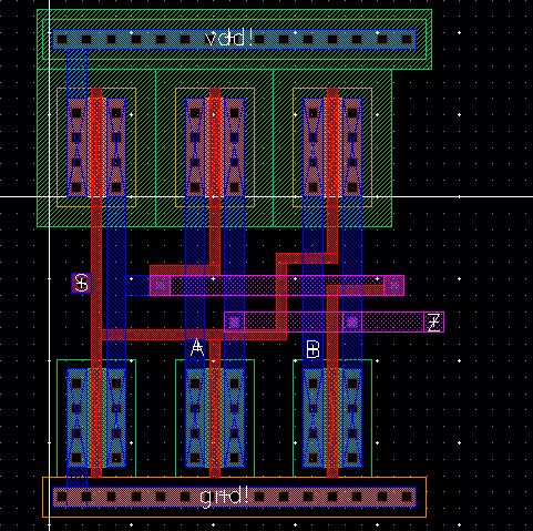
MUX
Full Adder
I used the full adder that I created from the previous lab.
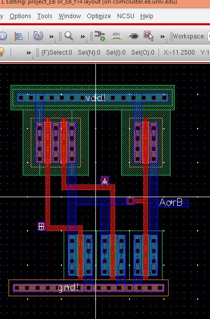
Once I created all the individual parts, I put them all together to create the following layout.
I made sure it LVS'd.
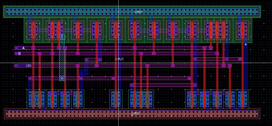
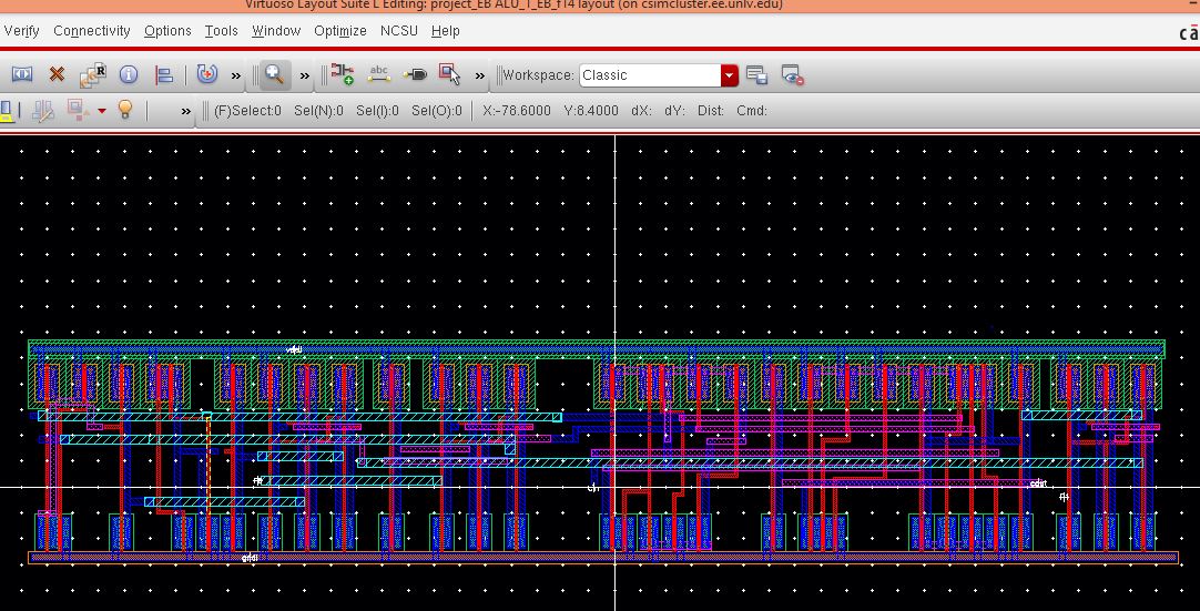
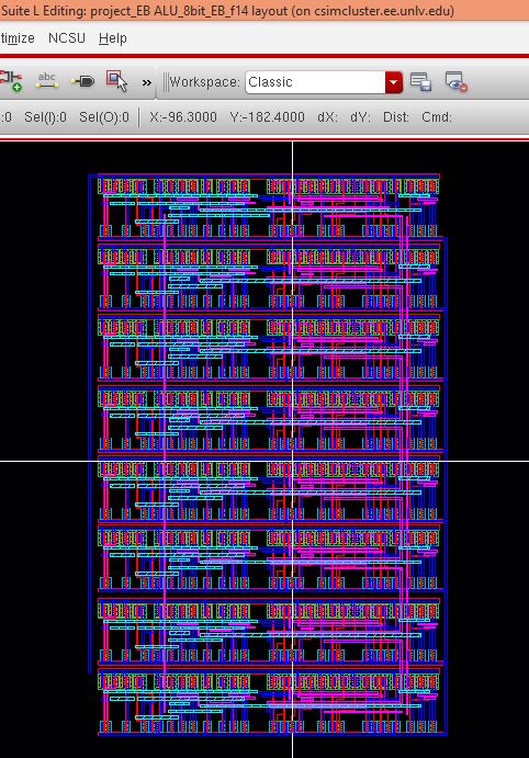
Now
that the 1 bit ALU was LVS'd i instantiated this layout 8 times. Edits
were needed to be made to get vdd and gnd to match up. Also the main
part of getting this to work was making sure to connect the cout of the
first adder to connect to the cin of the last adder..
Following is the layout of the 8 bit ALU.
This is the end of the project. You can find my zipped up cadence directory by clicking here.
The directory of my html page is found here.
I created zips of my folders and uploaded them to my google drive for back up.

Return to EE421 labs here.