Lab 8 - ECE 421L
MOSIS_chip2 jelib file (experimental results, posted May, 2014)
*100/2 PMOS
*Inverter made of 100/2 NMOS and PMOS
*61 stage ring oscillator using 10/2 MOSFETS
*20k n-well resistor
*20k hi-res poly resistor
*1k n+ resistor
*1k p+ resistor
*Bandgap reference
The following components were MISCELLANOUS for the lab:
* 4-bit Adder
Next we will discuss how to test each of the components on the chip.
NOTE!: Pin 20 on the chip is the dedicated ground (GND) pin for all the components that
will need to connect to ground, each component will have it's own VDD pin.
In addition, the entire chip has a vdd connection at pin 40. Connect this pin to vdd for
maximum ESD projection, otherwise leave floating.
Please only test one component at a time, do not have multiple VDD's connected to the
chip to test for example 3 resistors at a time just so their is no influence on your data results.
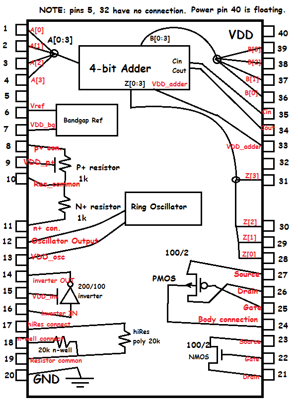
Below is the pin diagram of the chip.

100/2 NMOS
* For this component, their are various tests one can do depending on how far into the
course the student is. You have access to 3 pins as listed below:
DN - Drain connection (PIN 21)
GN - Gate connection (PIN 22)
SN - Source connection (PIN 23)
The body of the NMOS is directly connected to ground within the actual chip
TEST 1 - First lets connect a 5 volt source across the NMOS drain and source terminals.
Put 5 volts to the drain pin of the NMOS and put ground to the source pin of the NMOS.
Now connect the gate pin of the NMOS to ground. Since the gate is connected to ground,
the NMOS device should be OFF, meaning it is not conducting current. Carefully read
the current that flows into the drain pin of the NMOS with a multimeter, there should be
0 amps flowing.
TEST 2 - Now connect the gate pin of the NMOS to 5 volts and read the current flowing
through drain. This time you should see a current flowing in the microAmp range. At this
stage, the NMOS is fully ON.
TEST 3 - Keep the voltage across the drain and source at 5 volts, you might need a second
voltage source at this point. Connect the second voltage source to the gate pin of the
NMOS, make sure to connect the negative terminal to the circuits ground (pin 20!). Now
slowly vary the voltage source from 0 volts to 5 volts in steps of 100 mV, notice how the
current through the drain varies. Can you identify the threshold voltage of the NMOS
by simply sweeping the second voltage source until you go from no current flowing through
the drain to having current starting to flow?
100/2 PMOS
* For this component we will use very similar tests as the NMOS component above. For the
PMOS, you will have access to 4 pins as listed below:
DP - Drain connection (PIN 26)
GP - Gate connection (PIN 25)
SP - Source connection (PIN 27)
BP - Body Connection (PIN 24)
Notice that for the PMOS you have access to the body connection, this can allow you to
test for other parameters such as body effect (when the source and body are not tied to
the same node). If you are unfamiliar of what to do with this pin, CONNECT THE BODY
CONNECTION PIN TO VDD (5 volts).
TEST 1 - First lets connect a 5 volt source across the PMOS source and drain terminals.
Put 5 volts to the source pin of the PMOS and put ground to the drain pin of the PMOS.
Now connect the gate pin of the PMOS to ground. Since the gate is connected to ground,
the PMOS device should be ON, meaning it is conducting current. Carefully read
the current that flows into the source pin of the PMOS with a multimeter, there should be
a current in the microamps range flowing.
TEST 2 - Now connect the gate pin of the PMOS to 5 volts and read the current flowing
through source. This time you should see no current flowing, the PMOS is OFF.
TEST 3 - Keep the voltage across the source and drain at 5 volts, you might need a second
voltage source at this point. Connect the second voltage source to the gate pin of the
PMOS, make sure to connect the negative terminal to the circuits ground (pin 20!). Now
slowly vary the voltage source from 5 volts to 0 volts in steps of 100 mV, notice how the
current through the drain varies. Can you identify the threshold voltage of the PMOS
by simply sweeping the second voltage source until you go from no current flowing through
the drain to having current starting to flow?
200/100 INVERTER
* For this component we will use very similar tests as the NMOS component above. For the
PMOS, you will have access to 4 pins as listed below:
Out - Input (PIN 14)
VDD_inv - Input voltage for the inverter (Pin 15)
In - Output (Pin 16)
The ground for the inverters are connected within the chip itself, to pin 20.
Test 1 - Connect the VDD_inv pin to 5 volts, connect 5 volts to the Input pin and use a
multimeter to read the voltage at the output. Do you expect to read 0 volts?
Test 2 - Now change the voltage at the input to 0 volts and read the output voltage, is it
now at 5 volts?
61 stage ring oscillator
* For this component you have access to the following pins:
VDD_osc - The ring oscillator power supply (PIN 13)
Osc_out - Output of the ring oscillator (PIN 12)
The ground for the inverters in the oscillator are connected within the chip itself, to pin 20.
Test 1 - Apply 5 volts to the VDD_osc pin and use an oscilloscope to measure the output of the
ring oscillator at the Osc_out pin. You should see an imperfect square wave with a period
of about 5 to 20 ns. measure the period of your square wave.
Resistors
* For this stage of testing, we will use the same methods for all of the following four resistors.
*20k n-well resistor (left pin ->PIN19), (right pin -> PIN18)
*20k hi-res poly resistor (left pin ->PIN19), (right pin -> PIN17)
*1k n+ resistor (left pin -> PIN11), (right pin -> PIN10)
*1k p+ resistor (right pin -> PIN8), (N-well -> PIN 9), (left pin -> PIN 10)
Test 1 - Connect Pin19 to ground, we will first test out the 10k n-well resistor. Apply 5 volts to pin18
and measure the current flowing into the resistor with a multimeter. Using V = I*R, calculate the
resistance of the n-well resistor, it should be near 20k. Now remove the 5 volts and apply it to
pin17. Measure the current once again and do the same calculation, V = I*R to verify that the
20k hi-res poly resistor is near 20k as designed.
Test 2 - Connect pin10 to ground and Pin9 to 5 volts (do not worry abou the N-well connection at this
time). Apply 5 volts to Pin11 and measure the current flowing through that pin. Verify that the
resistance is 1k for the n+ resistor. Now apply that 5 volts to pin8 and measure the current that
flows through the resistor. Verify that the p+ resistor is also 1k.
Bandgap Reference
* For this component you have access to the following pins:
Vref - Voltage reference of 1.25 volts (PIN6)
VDD_bg - voltage source for the bandgap (PIN7)
Test 1 - Apply 5 volts to the VDD_bg pin to power up the bandgap. Now use a multimeter to
measure the output of the bandgap from pin Vref. You should read very close to 1.25 volts.
Test 2 - Now vary the voltage across the bandgap from 0 volts up to 6 volts in steps of 250
mV. At which voltages does the bandgap give a good 1.25 volt reading? Does it function
correctly when the VDD_bg source is below 3 volts?
4-bit Adder
A special note on this component. There are buffers on the output of this component
in order to drive large off-chip capacitances.
* For this component you have access to the following pins:
VDD_adder - Voltage source for the adder (PIN33)
Sum[0] - (PIN28) [this is the Least Significant Bit of the result Z]
Sum[1] - (PIN29)
Sum[2] - (PIN30)
Sum[3] - (PIN31)
Cout - (PIN34)
Cin - (PIN35)
B[0] - (PIN36) [this is the Least Significant Bit of input B]
B[1] - (PIN37)
B[2] - (PIN38)
B[3] - (PIN39)
A[0] - (PIN1) [this is the Least Significant Bit of input A]
A[1] - (PIN2)
A[2] - (PIN3)
A[3] - (PIN4)
Operation: The adder will add the two 4-bit words A and B (A + B = Z = Sum)
Test 1- Connect 5 volts to VDD_adder pin, test out the 4-bit adder by inputting
different combinations to the A[0:3] and B[0:3] pins. Use wires to tie each of
these inputs to either gnd or the 5 volt power supply rail to provide logical
"0" and "1". Read the result by using a multimeter and probing each output pin
from Sum[0] to Sum[1] as well as carry out. Can you figure out which bit
from the values A, B, and Sum is the most significant bit? Is it bit 0 or bit 3.
Below is the layout of the chip: