Lab 6 -
EE 421L
Authored
by Min Lan,
LANM2@UNLV.NEVADA.EDU
10/11/2013
Electric library: ML_ee421L_f13_lab6.jelib
Lab
description
In this lab, we will draft the schematics and layout for 2-input NAND gate, 2-input OR gate,
and XOR gate. After that we will use them to make a full adder. SPICE and IRSIM are used to
simulate their functionalities.
2-input NAND gate
Schematics
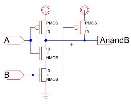
- Create a new schematic cell and copy a PMOS and an NMOS from jelib file for Lab 5
- Add power, ground, and off-page connectors
- Wire the components and export at the off-page connectors
- Make sure to choose the correct characteristics for the exports, A and B are inputs, AnandB is output
- Before we simulate the gate, let's create an icon view
- From the View menu, select Make Icon View
- If
the correct characteristics are set for the exports, you should see
inputs on the left, and outputs on the right (after deleting the
obstructing box)

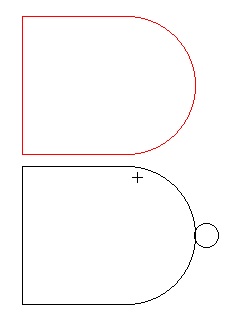
- Place a circle on the cell, from the Object Properties windows set the Degrees of the circle to 180˚
- Use opened-polygon for the body, and use a circle of size 1x1 as the bubble
- You can place a schematic elements on the {ic} cell for comparison

- Finally attach the exports (with arcs) to the main icon
- The Y-position of the exports (and arcs) should be exactly 1 unit
below/above the top/bottom borders of the icon; otherwise, the arc may
not align well when used as component in other cells.

- The icon view is done, press Control-U to go up to the schematic view
- Make sure to do DRC before simulation
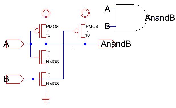
- Now, we can simulate the schematics
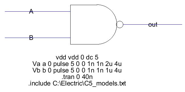
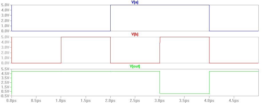

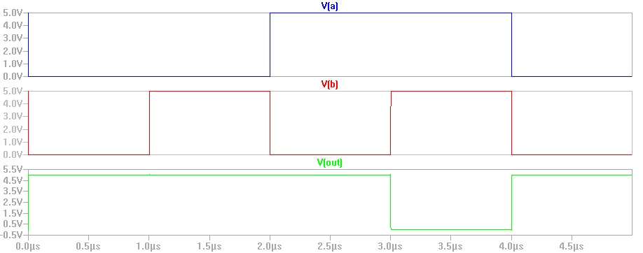
Output matches the NAND gate's truth table
Layout
- Create a layout cell with identical name, copy from the layout of 20/10 inverter from Lab 5
- Delete the arcs, change the Y-size of the PMOS group to 10, copy and place the components
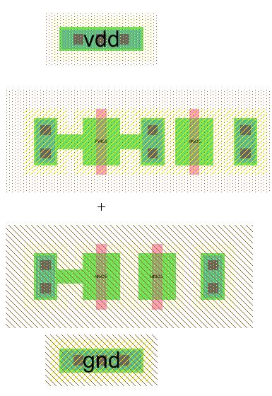
- Connect the Active Pins to the MOSFETs, bring the components together
- Adjust X-Sizes of the N-Well and P-Well pins to match the size of the layout
- Use Metal-1-Poly-1 contact to connect the polysilicons at the gate
- Use Metal-2-Metal-1 contacts to export the inputs and outputs
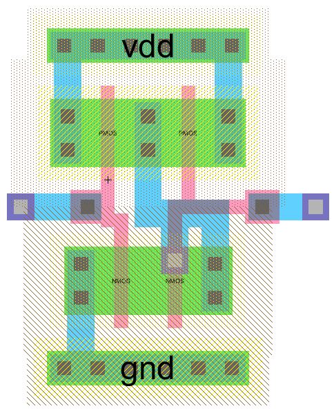
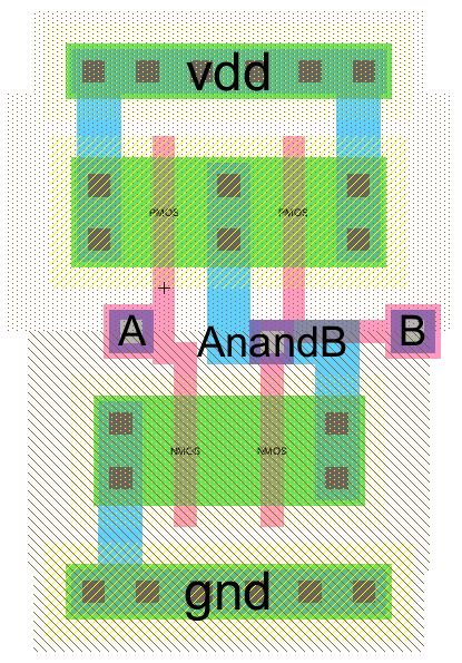
- Do DRC, LVS, Well Checks
- The Layout-Versus-Schematics check gives mismatch errors
- The NMOS tied to ground has B as its gate input, swapping the export will fix the problem


- Create a layout cell to simulate the layout
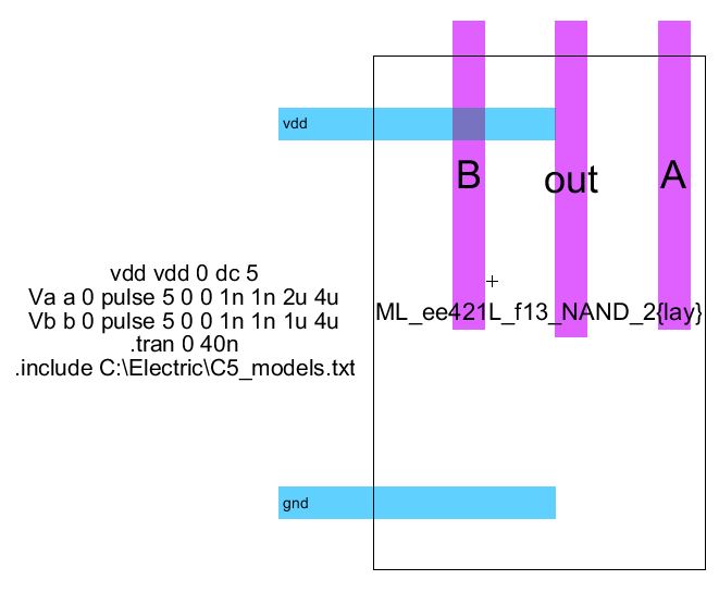
- To prevent the metals from overlapping, Metal-2 must be use to connect to the inputs and outputs
- Also, we must export vdd and gnd in the layout view, but not in schematic view


2-input NOR gate
Schematics
- Copy a PMOS and an NMOS from the NAND gate's schematic view
- Change the width of the PMOS to 20
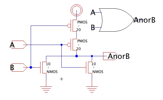
- Follow simular steps to wire the NOR gate, create an icon view for NOR gate

- DRC the schematic
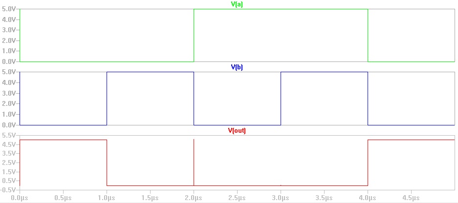
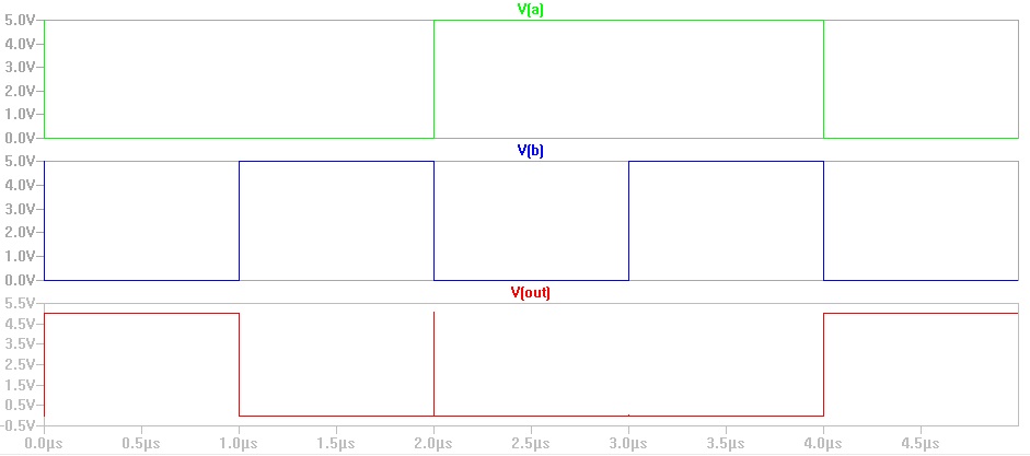
- Create a schematic cell (similar to simulation of NAND gate) to simulate the NOR gate


Layout
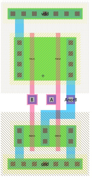
- Duplicate the layout view of NAND gate and named it so that the copy will be grouped with the schematic view of NOR gate
- Delete all the arcs and separate the MOSFETs and Active Pins
- Set the Width of the PMOS to 20, and Y-Size of the P-Act Pins to 20
- Note that now the NMOS group requires one extra N-Act Pin and the PMOS group have one extra P-Act, add one copy to the former, remove the extra from the latter.


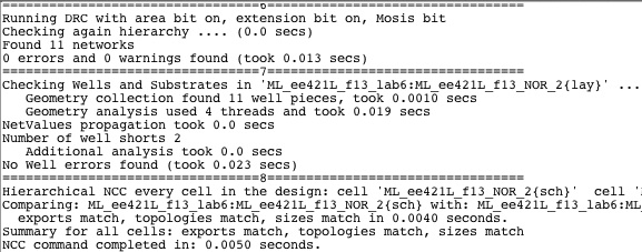
- Check the layout against NRC, LVS, Well-check.
- Create a new schematic to simulate with SPICE and IRSIM


XOR gate
Schematics
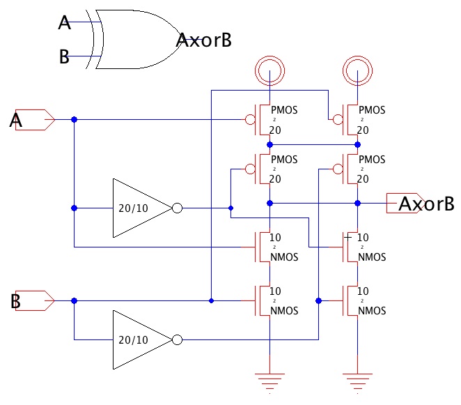
- Use Fig.12.18 to draft the schematics for XOR gate
- Note that the schematic require inverted A and B inputs, use inverters from Lab 5
- Note that the PMOS is 20/2 and the NMOS is 10/2

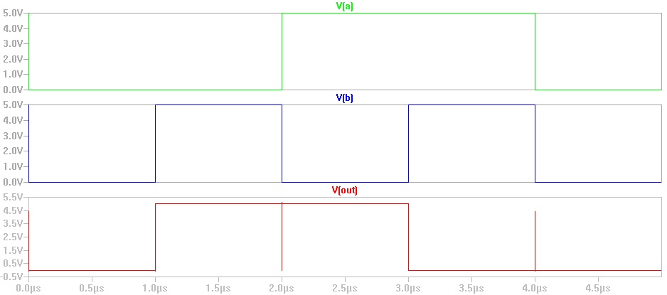
- Simulate the XOR gate and compare it with the truth table


Layout
- Similar to the schematics, drag two inverters into the layout for inverted A and B inputs
- Route the power and ground pins to the inverters

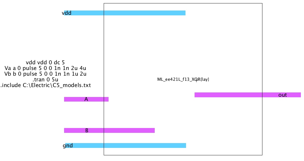
- Simulate the layout


Full Adder (1)
Schematics:
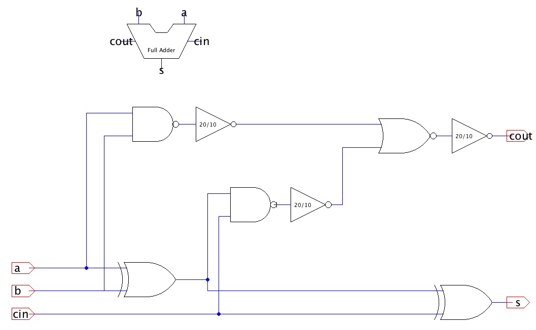
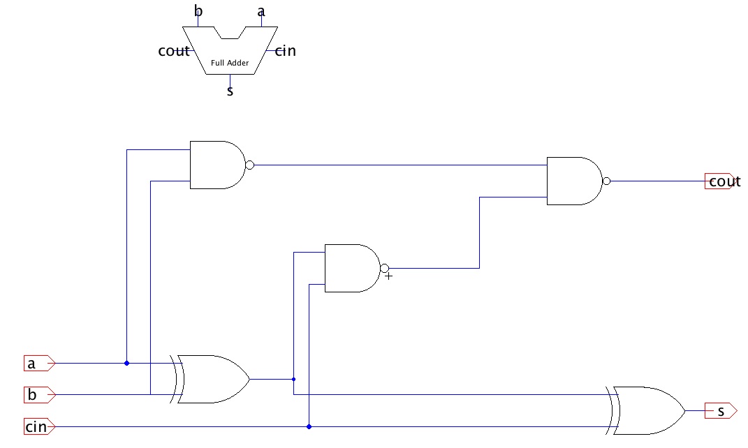
- Fig. fulladder

- Use NAND + inverter for AND gates, use NOR + inverter for the OR gate

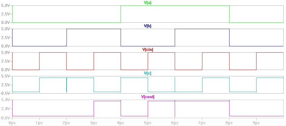
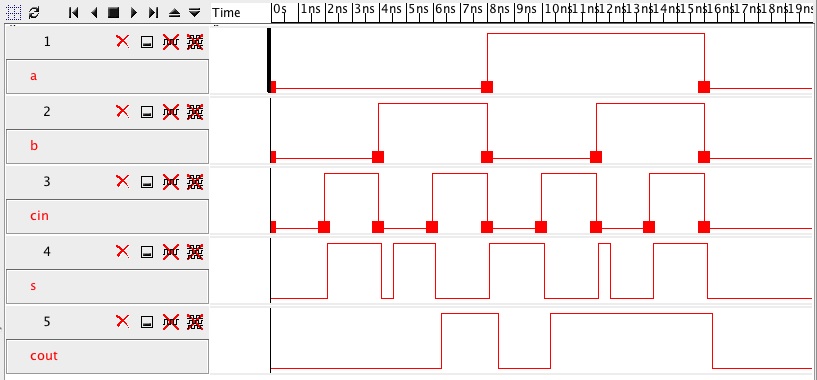
- Simulate the full adder and compare the result to the truth table


Full Adder (2)
Schematics:
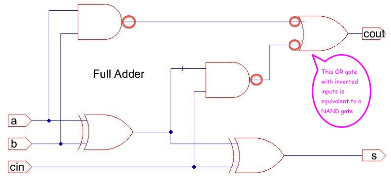
- Consider the following schematic
- If we place two inverters (bubbles) between the AND gates and the OR gate

- The adder will still function
- Recall from Logic Design I, an OR gate with both of its input inverted is equivalent to a NAND gate

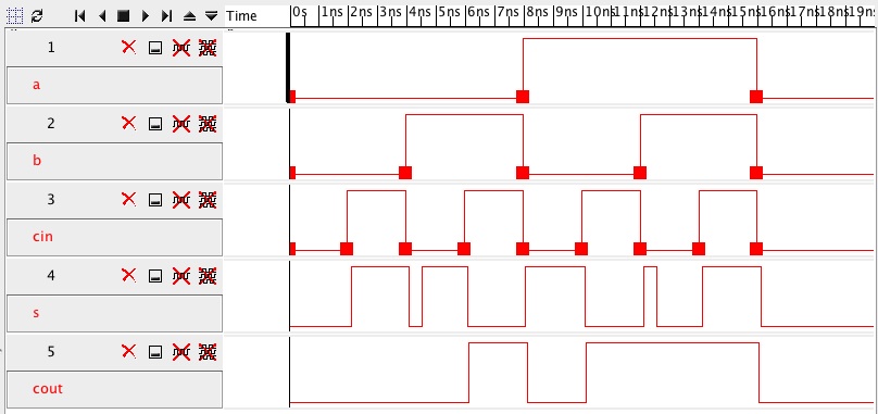
- To prove that the full adder functions, simulate it with SPICE and IRSIM


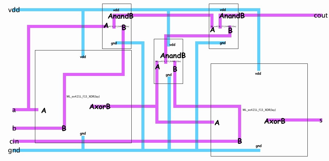
Layout:
- Use Metal-2 to connect inputs and outputs of the components
- Metal-1 cannot be used except to route vdd and gnd

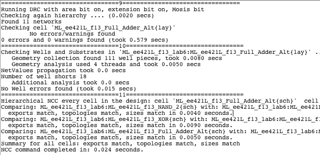
- DRC, NCC, ERC the layout

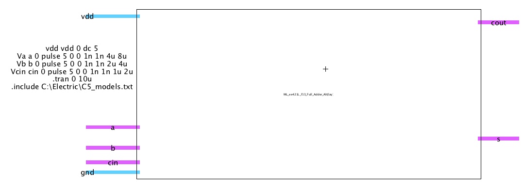
- Simulate and compare


Backup
Zip both your library file and your webpages and email to yourself.

Return to EE 421L Labs

